|
T(msec) = 41.12×m + 0.040 ×(m×q) + 2.85×n − 32.99. |
As with full frames, selecting a frame time
less than the most efficient value results in loss of observing efficiency.
Frame times are rounded up to the nearest 0.1 sec, and can range from 0.2 to
10.0 sec.
When operating with only one chip, subarrays as small as 100 rows are
allowed (this permits 0.3 sec frame times which pay no penalty in
dead time if q ≤ 200. Use the
above equation to determine what the most efficient frame time
is for the desired ACIS configuration.
For multichip observations, the smallest allowed number of
rows is 128. For small subarrays, the aiming uncertainties plus dither
should be taken into account; see Section 6.11 and
references therein.
Furthermore, S3-only observations are now required to include an FI chip, as detailed in
Section 6.20.
Table 6.5: CCD Frame Time (sec) for Standard Subarrays
| Subarray | ACIS-I (no. of chips)
| ACIS-S (no. of chips) |
| 1 | 6 | 11 | 2 | 6 |
| 1 | 3.0 | 3.2 | 3.0 | 3.0 | 3.2 |
| 1/2 | 1.5 | 1.8 | 1.5 | 1.6 | 1.8 |
| 1/4 | 0.8 | 1.2 | 0.8 | 0.9 | 1.1 |
| 1/8 | 0.5 | 0.8 | 0.4 | 0.5 | 0.7 |
| 1The minimum configurable selection for an ACIS-S3 observation is 2 chips, owing to the requirement to include at least one FI chip (Section 6.20)
|
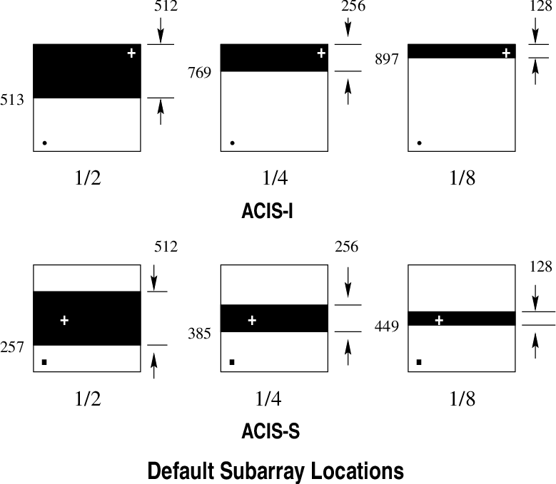 Figure 6.19: Examples of various subarrays. The heavy
dot in the lower left indicates the origin.
Trailed Images
It takes 40 μsec to transfer the charge from one row to another
during the process of moving the charge from the active region to the
frame store region. This has the interesting consequence that each
CCD pixel is exposed not only to the region of the sky at which the
observatory was pointing during the long (frame time) integration, but
also, for 40 μsec each, to every other region in the sky along
the column in which the pixel in question resides.
Figure 6.20 is an example where there are bright
features present so intense that the core of the PSF is suppressed
because of pile-up (see Section 6.16),
allowing the tiny contribution of the flux
due to trailing to be stronger than the (piled-up) core of the direct
exposure-hence the
trailed image is clearly visible. Trailed images are also referred to
as "read-out artifacts," "transfer smear," or "out-of-time images."
The user needs to be aware of this phenomenon as it has implications
for the data analysis, including estimates of the background.
In some cases, the
trailed image can be used to obtain an unpiled spectrum and can also
be used to perform 40 microsec timing analysis of (extremely bright)
sources.
Figure 6.19: Examples of various subarrays. The heavy
dot in the lower left indicates the origin.
Trailed Images
It takes 40 μsec to transfer the charge from one row to another
during the process of moving the charge from the active region to the
frame store region. This has the interesting consequence that each
CCD pixel is exposed not only to the region of the sky at which the
observatory was pointing during the long (frame time) integration, but
also, for 40 μsec each, to every other region in the sky along
the column in which the pixel in question resides.
Figure 6.20 is an example where there are bright
features present so intense that the core of the PSF is suppressed
because of pile-up (see Section 6.16),
allowing the tiny contribution of the flux
due to trailing to be stronger than the (piled-up) core of the direct
exposure-hence the
trailed image is clearly visible. Trailed images are also referred to
as "read-out artifacts," "transfer smear," or "out-of-time images."
The user needs to be aware of this phenomenon as it has implications
for the data analysis, including estimates of the background.
In some cases, the
trailed image can be used to obtain an unpiled spectrum and can also
be used to perform 40 microsec timing analysis of (extremely bright)
sources.
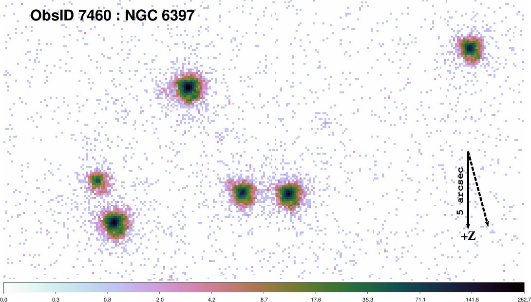
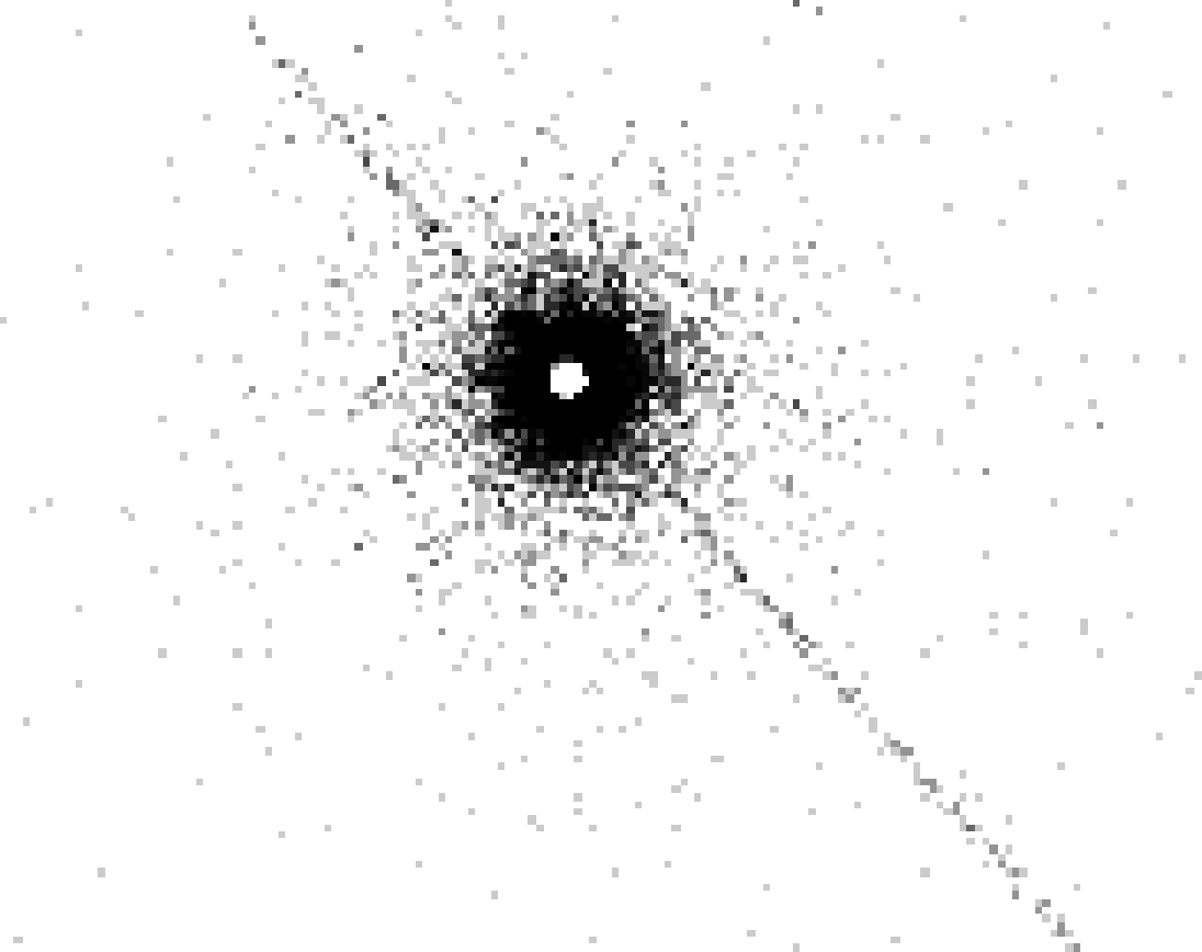 Figure 6.20: Trailed image of a strong X-ray
source. The core of the image is faint due to pile-up. Most events
here are rejected because of bad grades. The read-out direction is
parallel to the trail.
Figure 6.20: Trailed image of a strong X-ray
source. The core of the image is faint due to pile-up. Most events
here are rejected because of bad grades. The read-out direction is
parallel to the trail.
6.13.2 Alternating Exposures
In some instances, it is desirable to have both long and short frame times.
If the exposure time is made very short, pile-up may be
reduced, but the efficiency of the observation is greatly reduced by the
need to wait for the full 3.2 sec (if six chips are clocked) for the
frame-store array processing.
In alternating exposure mode, all CCDs are clocked in unison, but have
two exposure times. One (typically short) primary exposure of length
0.2 < tp < Topt sec is followed by k
secondary exposures of length ts (typically the standard optimal
time Topt, for instance, 3.2 sec if six chips are clocked
with full frames).
Permissible values of k range from 1 to 15.
The short exposures are used
to reduce photon pile-up, and the long exposures are useful for studying the fainter
objects in the field of view. For example, a typical choice of long and short exposure times might
be 3.2 and 0.3 sec. If k = 3, ACIS would perform a flush frame followed by one 0.3 sec
exposure, and then three exposures of 3.2 sec, repeating until the
total observing time expires.
If the duty cycle of long exposures is 1:k (primary:secondary), the observing
efficiency η is then
|
η = |
tp + k ts
tp + ( k + 1 ) ts
|
|
| (6.2) |
6.13.3 Continuous Clocking (CC) Mode
The continuous clocking mode is provided to allow 3 msec timing at the
expense of one dimension of spatial resolution. In this mode, one
obtains 1 pixel × 1024 pixel images, each with an integration time of
2.85 msec. Details as to the spatial distribution in the columns are
lost-other than that the event originated in the sky along the line
determined by the length of the column.
In the continuous clocking mode, data are continuously clocked through
the CCD and frame store. The instrument software accumulates data into
a buffer until a virtual detector of size 1024 columns by 512 rows is
filled. The event finding algorithm is applied to the data in this
virtual detector and 3×3 event islands are located and recorded to
telemetry in the usual manner (Section 6.15.1). This procedure has the advantage that
the event islands are functionally equivalent to data accumulated in
TE mode, hence differences in the calibration are minimal. The row
coordinate, called CHIPY in the Flexible Image Transport System (FITS) file, maps into time in that a
new row is read from the frame store to the buffer every 2.85 msec.
This does have some minor impacts on the data. For example, since the
event-finding algorithm is looking for a local maximum centered in a
3×3 pixel area, it cannot find
events on the edges of the virtual detector. Hence, CHIPX cannot be 1
or 1024, and CHIPY cannot be 1 or 512. In
other words, events cannot occur at certain times separated by
512×2.85 msec or 1.4592 sec. Likewise, it is impossible for two
events to occur in the same column in adjacent time bins.
Event files for continuous-clocking mode data contain two
time columns, TIME, and TIME_RO. The TIME_RO records
the read-out times (effectively the time the virtual frame
is processed to identify events). The TIME column is
an estimate of the photon time of arrival at the detector,
based on the read-out time, the aspect solution, and the
specified sky location of the source. See the
acis_process_events documentation for information
on the generation of these columns. In order to ensure
that the TIMEs are as accurate as possible, it is best to
specify the source location to better than 0.5 arcsec.
The read-out time can differ from the arrival time
by about 2.9 to 5.8 s, depending on the nominal location of the
source on the CCD and the dither of the spacecraft.
6.14 Bias Maps
In general, the CCD bias-the amplitude of the charge in each pixel in
the absence of external radiation-is determined at every change of instrumental parameters or setup when ACIS is in place at the focus of the
telescope. These bias maps have proven to be remarkably stable and are
automatically applied in routine data processing.
The bias maps for continuous-clocking mode observations can be
corrupted by cosmic rays. If a cosmic ray deposits a lot of charge in
most of the pixels in one or more adjacent columns, the bias values
assigned to these columns will be too large. As a result, some
low-energy events that would have been telemetered will not be
telemetered because they do not satisfy the minimum pulse height
criterion and the spectrum of a source in the affected columns will be
skewed to lower energies. The BI CCDs are relatively insensitive to
the problem. A bias algorithm was
implemented in Cycle 6 to mitigate the problem.
Occasionally a cosmic ray produces an artifact in a bias map. The pipelines
search for these artifacts, and, when found, replace the bias map with another
from the same epoch. Work is in progress to use long-term average bias maps,
either when there are artifacts in the observation-specific bias map, or
for all observations.
6.15 Event Grades and Telemetry Formats
6.15.1 Event Grades
In the first step in detecting X-ray events, the on-board processing
examines every pixel in the full bias-subtracted CCD image (even in
the continuous clocking mode (Section 6.13.3)) and selects
as events those with values that both exceed the event threshold and
are greater than all of their touching or neighboring pixels
(i.e., a local maximum in a 3×3 pixel detection island).
The pixel pattern, and thus the event grade,
is determined by which of the outer pixels in a 3×3 grid
centered on the initial pixel have values above the split-event
threshold. Depending on the grade, the data are then included in
the telemetry. On-board suppression of certain grades is used
to limit the telemetry bandwidth devoted to background events (see
Section 6.17.1).
The grade of an event is thus a code that identifies which pixels
within the 3×3 pixel island, centered on the local
charge maximum, are above certain amplitude thresholds. The thresholds
are listed in Table 6.2. Note that the local maximum
threshold differs for the FI and the BI CCDs. A "Rosetta Stone" to
help one understand the ACIS grade assignments is shown in
Figure 6.21, and the relationship to the Advanced Satellite for Cosmology and Astrophysics (ASCA) grading
scheme is given in Table 6.6.
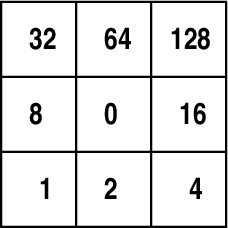 Figure 6.21: Schematic for determining
the grade of an event. The grade is determined by summing the numbers
for those pixels that are above their thresholds. For example, an
event that caused all pixels to exceed their threshold is grade 255. A
single pixel event is grade 0.
Table 6.6: ACIS flight grades and ASCA Grades
Figure 6.21: Schematic for determining
the grade of an event. The grade is determined by summing the numbers
for those pixels that are above their thresholds. For example, an
event that caused all pixels to exceed their threshold is grade 255. A
single pixel event is grade 0.
Table 6.6: ACIS flight grades and ASCA Grades
| ASCA grade
| ASCA grade
| |
| ACIS grades | CC mode graded | Other modes | Description |
| 0 | 0 | 0 | Single pixel |
| 64 65 68 69 | 2 | 2 | Vertical split up |
| 2 34 130 162 | 2 | 2 | Vertical split down |
| 8 12 136 140 | 3 | 3 | Horizontal split left |
| 16 17 48 49 | 4 | 4 | Horizontal split right |
| 72 76 104 108 | 6 | 6 | "L" & square, upper left |
| 10 11 138 139 | 6 | 6 | "L" & square, lower left |
| 18 22 50 54 | 6 | 6 | "L" & square, lower right |
| 80 81 208 209 | 6 | 6 | "L" & square, upper right |
| 1 4 32 128 | 1 | 1 | 2-pixel diagonal split |
| 5 33 132 160 | 1 | 1 | 3-pixel diagonal split |
| 36 129 | 1 | 1 | 3-pixel diagonal split |
| 37 133 161 164 | 1 | 1 | 4-pixel diagonal split |
| 165 | 1 | 1 | 5-pixel diagonal split |
| 3 6 9 20 | 5 | 5 | 3-pixel "L" with corner |
| 40 96 144 192 | 5 | 5 | 3-pixel "L" with corner |
| 13 21 35 38 | 5 | 5 | 4-pixel "L" with corners |
| 44 52 97 100 | 5 | 5 | 4-pixel "L" with corners |
| 131 134 137 145 | 5 | 5 | 4-pixel "L" with corners |
| 168 176 193 196 | 5 | 5 | 4-pixel "L" with corners |
| 53 101 141 163 | 5 | 5 | 5-pixel "L" with corners |
| 166 172 177 197 | 5 | 5 | 5-pixel "L" with corners |
| 24 | 7 | 7 | 3-pixel horizontal split |
| 66 | 2 | 7 | 3-pixel vertical split |
| 255 | 7 | 7 | All 9 pixels |
| All other grades | 7 | 7 | |
It is important to understand that most, if not all, calibrations of
ACIS are based on a specific subset of ACIS grades, called g02346. This
standard
set comprises ASCA grades 0,2,3,4, and 6. In the absence
of pile-up, this particular grade selection appears to optimize the
signal-to-background ratio, but this conclusion depends on the
detailed spectral properties of the source. Further, most of the
scientifically important characteristics of ACIS (effective area,
sensitivity, point spread function, energy resolution, etc.) are
grade- and energy-dependent.
6.15.2 Telemetry Formats
There are a number of telemetry formats available. Specifying a format
determines the type of information that is included in the telemetry
stream. The number of bits per event depends on which mode and which
format is selected. The number of bits per event, in turn, determines
the event rate at which the telemetry will saturate and data will be
lost until the on-board buffer empties. The formats available depend
on which mode (Timed Exposure or Continuous Clocking) is used. The
modes, associated formats, and approximate event rates at which the
telemetry saturates and one begins to limit the return of data, are
listed in Table 6.7. The formats are described in the
following paragraphs. Event "arrival time" is given relative to the
beginning of the exposure.
Table 6.7: Telemetry Saturation Limits
| Mode | Format | Bits/event | Events/sec* | Number of Events in full buffer |
| CC | Graded | 58 | 375.0 | 128,000 |
| CC | Faint | 128 | 170.2 | 58,099 |
| TE | Graded | 58 | 375.0 | 128,000 |
| TE | Faint | 128 | 170.2 | 58,099 |
| TE | Very Faint | 320 | 68.8 | 23,273 |
*(includes a 10% overhead for housekeeping data)
Faint
Faint format provides the event position in detector coordinates, an
arrival time, an event amplitude, and the amplitude of the signal in each pixel in the
3×3 event island
that determines the event grade. The bias map is telemetered
separately. Note that certain grades may be not be included in the
data stream (Section 6.17.1).
Graded
Graded format provides event position in detector coordinates, an
event amplitude, the arrival time, and the event grade. Note that
certain grades may be not be included in the data stream
(Section 6.17.1).
Very Faint
Very Faint (VF) format provides the event position in detector coordinates,
the event amplitude, an arrival time, and the pixel values in a 5×5
island. As noted in Table 6.7, this format is only
available with the Timed Exposure mode. Events are still graded by the
contents of the central 3×3 island. Note that certain grades may be
not be included in the data stream (Section 6.17.1). This
format offers the advantage of reduced background after ground processing
(see Section 6.17.2) for applicable observations with count rates sufficiently low as to avoid both telemetry saturation and event pile-up.
Studies (see
https://cxc.harvard.edu/cal/Acis/Cal_prods/vfbkgrnd)
of the ACIS background have shown that for
weak or extended sources, a significant reduction of background at low and high energies may be made by using the information from 5×5 pixel islands, i.e. very faint mode, instead of the faint mode 3×3 island. This screening results in a 1-2% loss of good events after ground processing. CIAO 2.2 and later provides a tool to utilize the VF mode for screening background events.
Please note that the Redistribution Matrix File (RMF) generation is the same for very faint mode
as it is for faint mode. See the "Why Topic"
https://cxc.harvard.edu/ciao/why/aciscleanvf.html.
The very faint mode screening also reduces the nonuniformity
of the non-X-ray background (see Section 6.17.1).
It is important to realize that VF mode uses more telemetry; the limit is ∼ 68.8 events/s (all telemetered grades), which includes the target flux and the full background
from all chips. Check the calibration web page
(https://cxc.harvard.edu/cal/Acis/Cal_prods/bkgrnd/current/background.html)
for a discussion of
background flares and the telemetry limit. In particular, review
Section 1.3 of the memo "General discussion of the quiescent and
flare components of the ACIS background" by M. Markevitch.
Starting with Cycle 11, the default upper energy
cutoff has been decreased from 15 keV to 13 keV.
To reduce the total background rate and the likelihood of
telemetry saturation, VF mode observers should consider using no more than 4 CCDs and an energy filter with a 12 keV upper cutoff.
If the target is brighter than 5-10 cts/s, either turning off more chips or using Faint mode may be necessary, depending on the total telemetered background included
for the operating chips (see Table 6.10).
See Section 6.22.1
for more information on selection of required and optional CCDs.
Pile-Up results when two or more photons are detected as a single
event. The fundamental impacts of pile-up are: (1) a distortion of the
energy spectrum-the apparent energy is approximately the sum of two
(or more) energies; and (2) an underestimate as to the correct
counting rate-two or more events are counted as one. A simple
illustration of the effects of pile-up is given in Figure
6.22. There are other, somewhat more subtle, impacts
discussed below (Section 6.16.1).
The degree to which a source will be piled can be roughly estimated
using PIMMS. Somewhat more quantitative estimates can be obtained
using the pile-up models in XSPEC, Sherpa, and the Interactive Spectral Interpretation System (ISIS). If the
resulting degree of pile-up appears to be unacceptable given the
objectives, then the proposer should employ some form of pile-up
mitigation (Section 6.16.3) as part of the observing
strategy. In general, pile-up should not be a problem in the
observation of extended objects, the Crab Nebula being a notable
exception, unless the source has bright knots or filaments.
 Figure 6.22: The effects of pile-up at 1.49
keV (Al Kα) as a function of source intensity. Data were taken
during HRMA-ACIS system level calibration at the XRCF. Single-photon
events are concentrated near the pulse height corresponding to the Al
Kα line ( ∼ 380 ADU), and events with 2 or more photons
appear at integral multiples of the line energy.
Figure 6.22: The effects of pile-up at 1.49
keV (Al Kα) as a function of source intensity. Data were taken
during HRMA-ACIS system level calibration at the XRCF. Single-photon
events are concentrated near the pulse height corresponding to the Al
Kα line ( ∼ 380 ADU), and events with 2 or more photons
appear at integral multiples of the line energy.
6.16.1 Other Consequences of Pile-Up
There are other consequences of pile-up in addition to the two
principal features of spurious spectral hardening and underestimating
the true counting rate by under counting multiple events. These
additional effects are grade migration and pulse saturation, both of
which can cause distortion of the apparent PSF.
Grade migration
Possibly the most troubling effect of pile-up is that the grade
distribution for X-ray events may change. The change of
grade introduced by pile-up has come to be referred to as "grade
migration." Table 6.8 shows an example of grade
migration due to pile-up as the incident flux is increased. In this
simple test, which involved only mono-energetic photons, the largest
effect is the depletion of G0 events and the increase of G7 events.
In general, as the incident flux rate increases, the fraction of the
total number of events occupying a particular event grade changes as
photon-induced charge clouds merge and the resulting detected events
"migrate" to other grades which are not at all necessarily included
in the standard (G02346) set. If one applies the standard
calibration to such data, the true flux will be under-estimated.
Table 6.8: ASCA Grade Distributions for different incident fluxes at 1.49
keV (Al Kα, based on data taken at the XRCF during ground
calibration using chip I3)
| Incident Flux* | G0 | G1 | G2 | G3 | G4 | G5 | G6 | G7 |
| 9 | 0.710 | 0.022 | 0.122 | 0.053 | 0.026 | 0.009 | 0.024 | 0.035 |
| 30 | 0.581 | 0.057 | 0.132 | 0.045 | 0.043 | 0.039 | 0.029 | 0.073 |
| 98 | 0.416 | 0.097 | 0.127 | 0.052 | 0.050 | 0.085 | 0.064 | 0.108 |
| 184 | 0.333 | 0.091 | 0.105 | 0.040 | 0.032 | 0.099 | 0.077 | 0.224 |
*arbitrary units
Pulse Saturation
One consequence of severe instances of pile-up is the creation of a
region with no events! In this case, the pile-up is severe enough that
the total amplitude of the event is larger than the on-board threshold
(typically 13 keV) and is rejected. Holes in the image can also be
created by grade migration of events into ACIS grades (e.g. 255) that
are filtered on-board.
PSF distortion
Obviously the effects of pile-up are most severe when the flux is highly
concentrated on the detector. Thus, the core of the PSF suffers more
from pile-up-induced effects than the wings. Figure 6.23
illustrates this point.
Because the core is suppressed, the PSF profile
appears less peaked and (apparently) broader than would be the case
if pile-up were negligible.
6.16.2 Pile-Up Estimation
It is clearly important in preparing a Chandra observing proposal to
determine if the observation will be impacted by pile-up, and if so,
to decide what to do about it (or convince the peer review why the
specific objective can be accomplished without doing anything). There
are two approaches to estimating the impact of pile-up on the
investigation. The most sophisticated uses the pile-up models in
XSPEC, Sherpa, and ISIS to create a simulated data set which can be
analyzed in the same way as real data. A less sophisticated,
but very useful, approach is to use the web version of PIMMS to
estimate pile-up, or to use Figures 6.23 and
6.24.
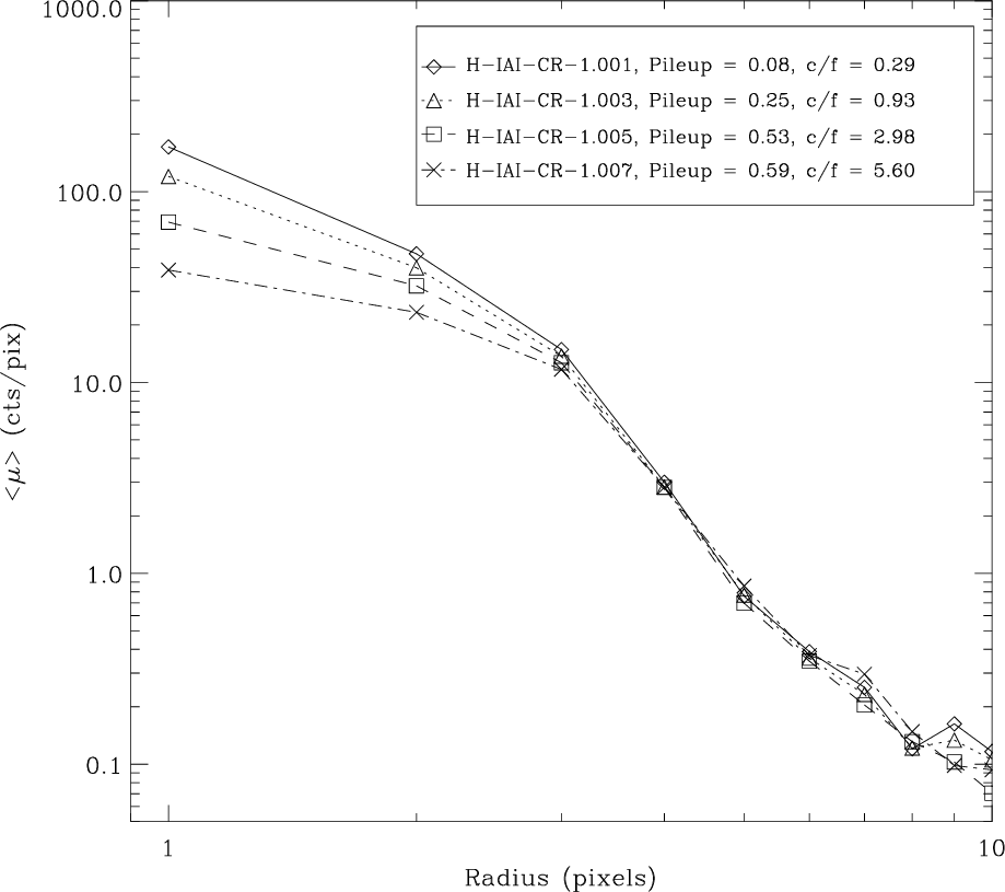 Figure 6.23: The effects of pile-up on the radial
distribution of the PSF are illustrated. These data were
taken during ground calibration at the XRCF. The specific "OBSIDs,"
the counting rate per CCD frame ("c/f"), and the "pile-up fraction"
as defined in Section 6.16.2 are given in the inset.
Figure 6.23: The effects of pile-up on the radial
distribution of the PSF are illustrated. These data were
taken during ground calibration at the XRCF. The specific "OBSIDs,"
the counting rate per CCD frame ("c/f"), and the "pile-up fraction"
as defined in Section 6.16.2 are given in the inset.
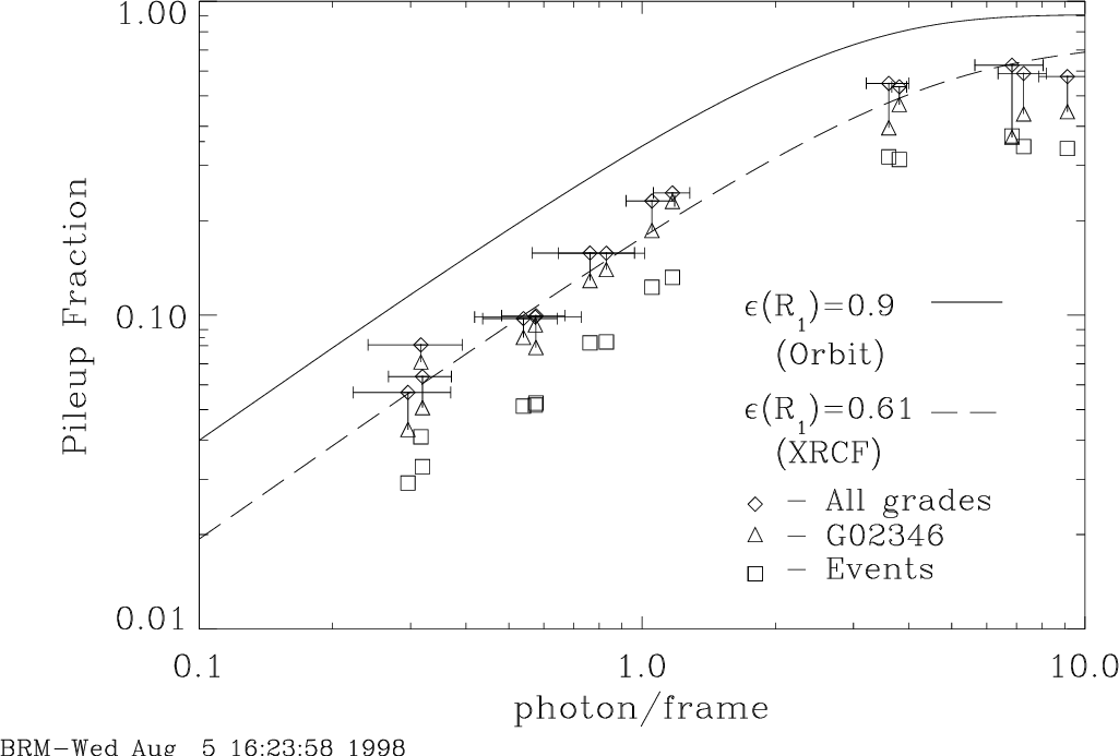 Figure 6.24: The pile-up fraction as a
function of the the counting rate (in the absence of pile-up in units
of photons/frame). The solid line is for on-orbit, the dashed line and
the data points are for, and from, ground-based data respectively. The
difference between the ground and flight functions are a consequence
of the improved PSF on-orbit, where gravitational effects are
negligible-see Chapter 4. Note that when pile-up occurs
there are two or more photons for each event, so the fraction of
events with pile-up is always less than the fraction of photons with
pile-up.
Figure 6.24: The pile-up fraction as a
function of the the counting rate (in the absence of pile-up in units
of photons/frame). The solid line is for on-orbit, the dashed line and
the data points are for, and from, ground-based data respectively. The
difference between the ground and flight functions are a consequence
of the improved PSF on-orbit, where gravitational effects are
negligible-see Chapter 4. Note that when pile-up occurs
there are two or more photons for each event, so the fraction of
events with pile-up is always less than the fraction of photons with
pile-up.
 Figure 6.25: MARX simulations of the effect of pile-up on the shape of the spectrum.
The true (solid line) and the detected (dotted line) spectra are shown for
four different viewing angles. The corresponding "pile-up fractions"-see Section 6.16.2-are 46%, 40%, 15%, and 2% as
the image is moved progressively further off-axis.
Simple Pile-Up Estimates
The pile-up fraction is the ratio of the number of detected events that
consist of more than one photon to the total number of detected
events. An estimate of the pile-up fraction can be determined from
Figure 6.24. The algorithm parametrizes the
HRMA+ACIS PSF in terms of the fraction of encircled energy that
falls within the central 3×3 pixel event detection cell, and assumes that the remaining energy is uniformly
distributed among the 8 surrounding 3×3 pixel detection
cells. The probabilities of single- and multiple-photon events are
calculated separately for the central and surrounding detection cells
and subsequently averaged (with appropriate weighting) to obtain the
pile-up fraction as a function of the true count rate-the solid
line in Figure 6.24. The model was tested against data
taken on the ground under controlled conditions-also shown in
Figure 6.24.
As a general guideline, if the estimated pile-up fraction is > 10%,
the proposed observation is very likely to be impacted. The first
panel (upper left) in Figure 6.25 qualitatively
illustrated the effect on a simulated astrophysical X-ray spectrum.
However, the degree of pile-up that is acceptable will depend
on the particular scientific goals of the
measurement, and there is no clear-cut tolerance level. If one's
scientific objective demands precise flux calibration, then the pile-up
fraction should probably be kept well below 10%.
The PIMMS tool provides the pile-up fraction using the algorithm
described here, both for direct observation with ACIS and also for
the zeroth-order image when a grating is inserted.
Simulating Pile-Up
John Davis developed an algorithm for modeling the effects
of pile-up on ACIS spectral data. The algorithm has been implemented
as of XSPEC V11.1 and Sherpa V2.2. The algorithm can be used to
attempt to recover the underlying spectrum from a source, or to
simulate the effects of pile-up for proposal purposes.
The algorithm has been tested by comparing CCD spectra with grating
spectra of the same sources. Care should be taken in applying the
algorithm-for example, using the appropriate regions for extracting
source photons and avoiding line-dominated sources. A description of
the algorithm can be found in Davis 2001 (Davis, J.E. 2001, ApJ, 562,
575). Details on using the algorithm in Sherpa are given in a
Sherpa "thread" as of CIAO V2.2 on the CXC CIAO web page:
https://cxc.harvard.edu/ciao/.
Figure 6.25: MARX simulations of the effect of pile-up on the shape of the spectrum.
The true (solid line) and the detected (dotted line) spectra are shown for
four different viewing angles. The corresponding "pile-up fractions"-see Section 6.16.2-are 46%, 40%, 15%, and 2% as
the image is moved progressively further off-axis.
Simple Pile-Up Estimates
The pile-up fraction is the ratio of the number of detected events that
consist of more than one photon to the total number of detected
events. An estimate of the pile-up fraction can be determined from
Figure 6.24. The algorithm parametrizes the
HRMA+ACIS PSF in terms of the fraction of encircled energy that
falls within the central 3×3 pixel event detection cell, and assumes that the remaining energy is uniformly
distributed among the 8 surrounding 3×3 pixel detection
cells. The probabilities of single- and multiple-photon events are
calculated separately for the central and surrounding detection cells
and subsequently averaged (with appropriate weighting) to obtain the
pile-up fraction as a function of the true count rate-the solid
line in Figure 6.24. The model was tested against data
taken on the ground under controlled conditions-also shown in
Figure 6.24.
As a general guideline, if the estimated pile-up fraction is > 10%,
the proposed observation is very likely to be impacted. The first
panel (upper left) in Figure 6.25 qualitatively
illustrated the effect on a simulated astrophysical X-ray spectrum.
However, the degree of pile-up that is acceptable will depend
on the particular scientific goals of the
measurement, and there is no clear-cut tolerance level. If one's
scientific objective demands precise flux calibration, then the pile-up
fraction should probably be kept well below 10%.
The PIMMS tool provides the pile-up fraction using the algorithm
described here, both for direct observation with ACIS and also for
the zeroth-order image when a grating is inserted.
Simulating Pile-Up
John Davis developed an algorithm for modeling the effects
of pile-up on ACIS spectral data. The algorithm has been implemented
as of XSPEC V11.1 and Sherpa V2.2. The algorithm can be used to
attempt to recover the underlying spectrum from a source, or to
simulate the effects of pile-up for proposal purposes.
The algorithm has been tested by comparing CCD spectra with grating
spectra of the same sources. Care should be taken in applying the
algorithm-for example, using the appropriate regions for extracting
source photons and avoiding line-dominated sources. A description of
the algorithm can be found in Davis 2001 (Davis, J.E. 2001, ApJ, 562,
575). Details on using the algorithm in Sherpa are given in a
Sherpa "thread" as of CIAO V2.2 on the CXC CIAO web page:
https://cxc.harvard.edu/ciao/.
6.16.3 Reducing Pile-Up
Various methods that can be used to reduce pile-up are summarized in this
section.
- • Shorten exposure time:
- By cutting back on CCD exposure time,
the probability of pile-up decreases. The user is advised to select the
best combination of a subarray and frame time to avoid losing
data as discussed in Section 6.13.1.
- • Use the Alternating Exposure option:
- This option simply
alternates between exposures that are subject to pile-up and those that
are not. The capability was originally developed for use with certain
grating observations to allow one to spend some time obtaining useful
data from a zeroth order image, which would otherwise be piled up.
See Section 6.13.2.
- • Use CC mode
- If two-dimensional imaging is not required,
consider using CC mode (Section 6.13.3).
- • Insert a transmission grating:
- Inserting either
the HETG (Chapter 8) or the
LETG (Chapter 9) will
significantly decrease the counting rate as the efficiency is
lower. The counting rate in the zero order image may then be low
enough to avoid pile-up.
- • Offset point:
- Performing the observation with the source
off-axis spreads out the flux and thus decreases the probability of
pile-up at the price of a degraded image. Figure 6.25
illustrated the impact.
- • Defocus:
- The option is only listed for completeness, the option
is not recommended or encouraged.
6.17 On-Orbit Background
There are three components to the on-orbit background. The first is
that due to the cosmic X-ray background (a significant fraction of
which resolves into discrete sources during an observation with
Chandra). The second component is commonly referred to as the charged
particle background. This arises both from charged particles,
photons, and other neutral particle interactions that ultimately deposit
energy in the instrument. The third component is the "read-out
artifact" which is a consequence of the "trailing" of the target
image during the CCD read-out; it is discussed in
Section 6.13.1.
The background rates differ between the BI and the FI chips, in
part because of differences in the efficiency for identifying charged
particle interactions. Figure 6.26 illustrates why.
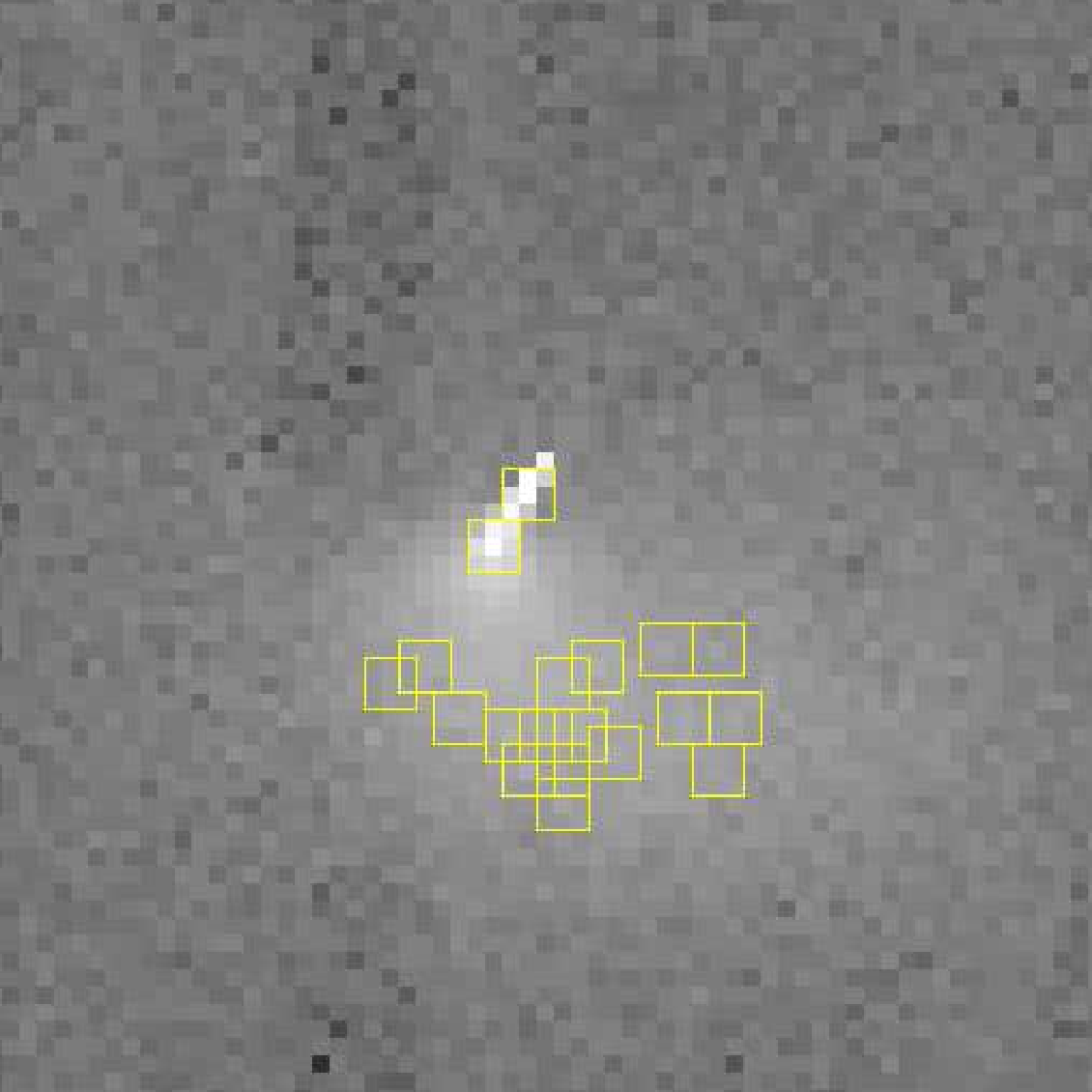
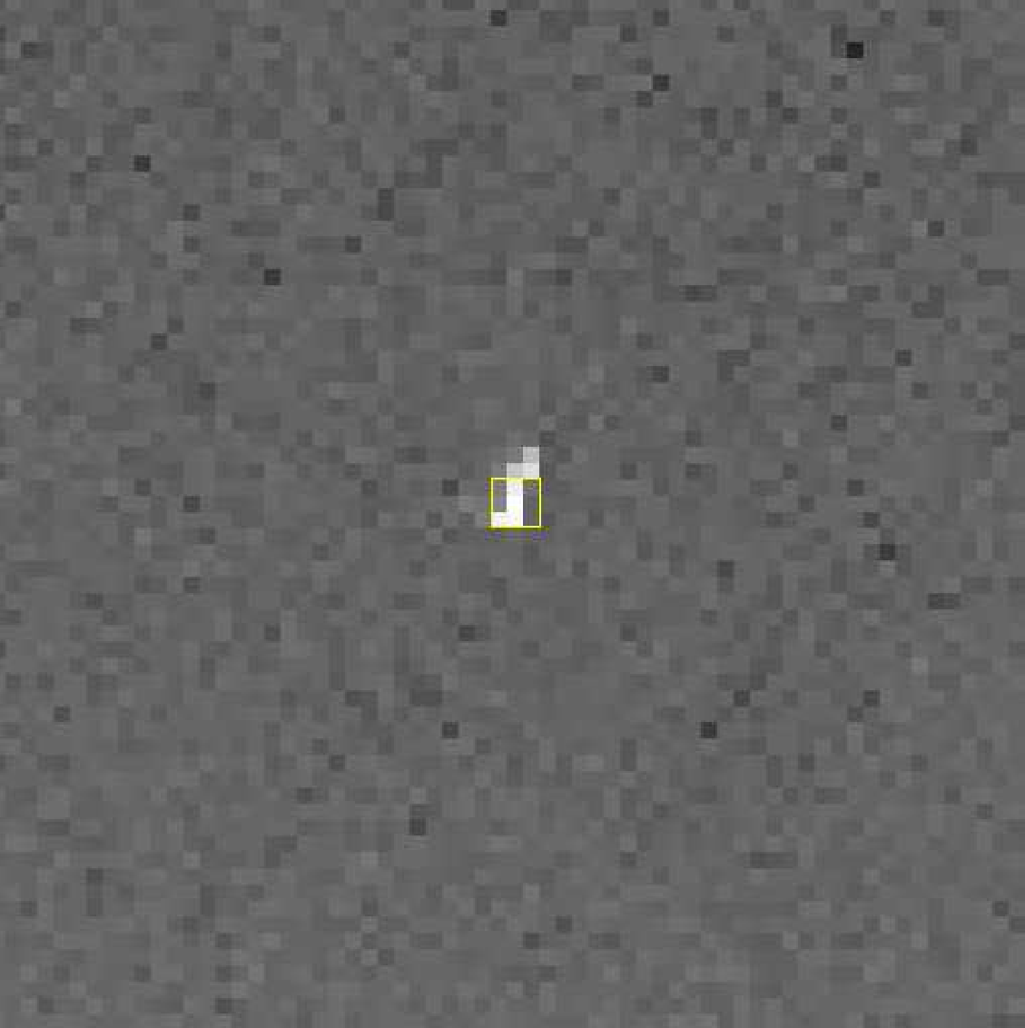 Figure 6.26: Enlarged view of an area of a FI chip I3 (left) and
a BI chip (right) after being struck by a charged particle. There is far
more "blooming" in the FI image since the chip is thicker. The
overlaid 3×3 detection cells indicate that the particle impact on the
FI chip produced a number of events, most of which end up as
ASCA Grade 7, and are thus rejected with high efficiency. The equivalent
event in the BI chip, is much more difficult to distinguish from an
ordinary X-ray interaction, and hence the rejection efficiency is
lower.
Figure 6.26: Enlarged view of an area of a FI chip I3 (left) and
a BI chip (right) after being struck by a charged particle. There is far
more "blooming" in the FI image since the chip is thicker. The
overlaid 3×3 detection cells indicate that the particle impact on the
FI chip produced a number of events, most of which end up as
ASCA Grade 7, and are thus rejected with high efficiency. The equivalent
event in the BI chip, is much more difficult to distinguish from an
ordinary X-ray interaction, and hence the rejection efficiency is
lower.
6.17.1 The Non-Celestial X-ray Particle Background
Beginning in 2002-Sep
and continuing until 2012-Jun,
observations have been carried
out with the ACIS in the stowed position, shielded from the sky by
the SIM structure, and collecting data in normal imaging TE VF mode at
−120 °C. Chips I0, I2, I3, S1, S2,
S3 were exposed. The SIM position was chosen so that the on-board calibration
source did not illuminate the ACIS chips.
This allowed characterization of the non-celestial contribution to X-ray background (i.e., of the effects of charged particles).
The resulting spectra from different
chips are shown in Figure 6.27. Chip S2 is similar
to the ACIS-I chips (denoted I023 in the figure) and not
shown for clarity.
In addition, in July-September 2001, Chandra performed several short
observations of the dark Moon, which blocks the cosmic X-ray background.
The dark Moon and stowed background spectra were indistinguishable
(except for short periods of flares and variable Oxygen line emission
in the Moon observations).
No background flares have been observed
in the stowed position. Thus, the ACIS-stowed background is a good
representation of the quiescent non-X-ray background in the normal
focal position and can be used for science observations.
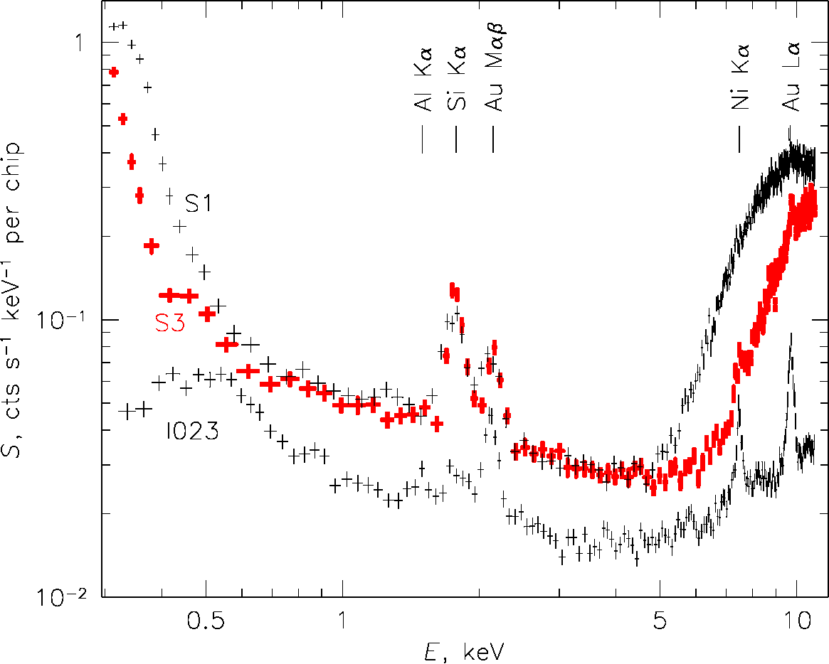 Figure 6.27: Energy spectra of the charged
particle ACIS background with ACIS in the stowed position (a 50 ks
exposure taken in 2002-Sep; standard grade filtering, no VF
filtering). Line features are due to particle-induced fluorescence of
material in and surrounding the focal plane. The "I023" points are from
combined I0, I2, and I3 data.
The flight-grade distributions in early measurements of the non-X-ray
background for the two types of CCDs are shown in
Figure 6.28. Although subsequent to these early
measurements the CCD temperature has been lowered and the
FI devices suffered the effects of the radiation damage, the
background is still dominated by the same grades. Based on these data,
events from flight grades 24, 66, 107, 214, and 255 are routinely
discarded on-board. The total rate of the discarded events is
available in the data stream. The remaining non-X-ray events
telemetered to the ground are still dominated (70-95%) by other bad
grades. They are not discarded on-board because some of them may turn
out to be valid X-ray events after ground processing.
For data taken using the VF telemetry format
(Section 6.15.2), the non-X-ray background can be reduced
in data processing by screening out events with significant flux in
border pixels of the 5×5 event islands. This screening leaves the data
from faint sources essentially the same while reducing
the FI background at different energies: a factor of
1.4 (E > 6 keV);
1.1 (1−5 keV); and
2 (near ∼ 0.5 keV).
For the BI chips the reductions are:
1.25 (E > 6 keV);
1.1 (1−5 keV); and
3 (near 0.3 keV).
In addition, the spatial nonuniformity of the non-X-ray background may
be reduced by VF screening; see the background uniformity memo at
https://cxc.harvard.edu/cal/Acis/detailed_info.html#background.
The screening
algorithm has been incorporated into the CIAO tool
acis_process_events. Further discussion may be found at
https://cxc.harvard.edu/cal/Acis/Cal_prods/vfbkgrnd/index.html.
Proposers should be aware that telemetry saturation occurs at lower
count rates for observations using the VF format, so they may need to
take steps to limit the total ACIS count rate (see
Section 6.17.2). Proposers should also be aware that if there
are bright point sources in the field of view, the screening criterion
discussed above is more likely to remove source events due to pile-up
of the 5×5 pixel event islands. Point sources should have count rates
significantly less than 0.1 cts/sec to be unaffected. However, there
is no intrinsic increase of pile-up in VF data compared to Faint mode,
and the screening software can be selectively applied to regions,
excluding bright point-like sources. Thus the use of VF mode is
encouraged whenever possible.
Figure 6.27: Energy spectra of the charged
particle ACIS background with ACIS in the stowed position (a 50 ks
exposure taken in 2002-Sep; standard grade filtering, no VF
filtering). Line features are due to particle-induced fluorescence of
material in and surrounding the focal plane. The "I023" points are from
combined I0, I2, and I3 data.
The flight-grade distributions in early measurements of the non-X-ray
background for the two types of CCDs are shown in
Figure 6.28. Although subsequent to these early
measurements the CCD temperature has been lowered and the
FI devices suffered the effects of the radiation damage, the
background is still dominated by the same grades. Based on these data,
events from flight grades 24, 66, 107, 214, and 255 are routinely
discarded on-board. The total rate of the discarded events is
available in the data stream. The remaining non-X-ray events
telemetered to the ground are still dominated (70-95%) by other bad
grades. They are not discarded on-board because some of them may turn
out to be valid X-ray events after ground processing.
For data taken using the VF telemetry format
(Section 6.15.2), the non-X-ray background can be reduced
in data processing by screening out events with significant flux in
border pixels of the 5×5 event islands. This screening leaves the data
from faint sources essentially the same while reducing
the FI background at different energies: a factor of
1.4 (E > 6 keV);
1.1 (1−5 keV); and
2 (near ∼ 0.5 keV).
For the BI chips the reductions are:
1.25 (E > 6 keV);
1.1 (1−5 keV); and
3 (near 0.3 keV).
In addition, the spatial nonuniformity of the non-X-ray background may
be reduced by VF screening; see the background uniformity memo at
https://cxc.harvard.edu/cal/Acis/detailed_info.html#background.
The screening
algorithm has been incorporated into the CIAO tool
acis_process_events. Further discussion may be found at
https://cxc.harvard.edu/cal/Acis/Cal_prods/vfbkgrnd/index.html.
Proposers should be aware that telemetry saturation occurs at lower
count rates for observations using the VF format, so they may need to
take steps to limit the total ACIS count rate (see
Section 6.17.2). Proposers should also be aware that if there
are bright point sources in the field of view, the screening criterion
discussed above is more likely to remove source events due to pile-up
of the 5×5 pixel event islands. Point sources should have count rates
significantly less than 0.1 cts/sec to be unaffected. However, there
is no intrinsic increase of pile-up in VF data compared to Faint mode,
and the screening software can be selectively applied to regions,
excluding bright point-like sources. Thus the use of VF mode is
encouraged whenever possible.

 Figure 6.28: Fraction of ACIS background events as a function of grade from
early in-flight data for an FI chip (S2; top) and a BI chip (S3; bottom).
Figure 6.28: Fraction of ACIS background events as a function of grade from
early in-flight data for an FI chip (S2; top) and a BI chip (S3; bottom).
6.17.2 The Total Background
In sky observations, two more components to the background come into
play. The first is the cosmic X-ray background which, for moderately
long ( ∼ 100 ks) observations, will be mostly resolved into discrete
sources (except for the diffuse component below 1 keV) but,
nevertheless, contributes to the overall counting rate. The second is
a time-variable "flare" component caused by any charged particles
that may forward-scatter from the HRMA mirrors and have sufficient
momentum so as not to be diverted from the focal plane by the
magnets included in the observatory for that purpose, or
from secondary particles (Section 6.17.3).
Figure 6.29 compares flare-free
ACIS-S3 spectra of the non-X-ray (dark Moon) background and a
relatively deep pointing to a typical region of the sky away from
bright Galactic features.
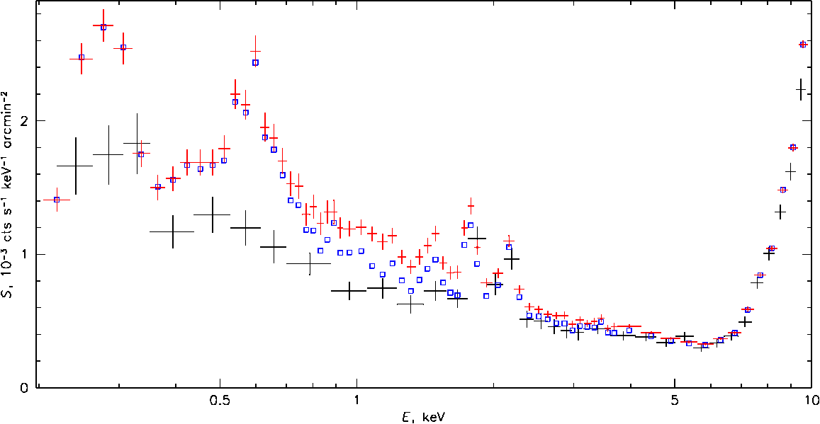 Figure 6.29: ACIS-S3
spectrum of the non-X-ray background (large
crosses) overlaid on the quiescent blank sky spectrum. Small
crosses show the total sky spectrum, while squares show the
diffuse component left after the exclusion of all point
sources detectable in this 90 ks exposure. Standard grade
filtering and VF filtering are applied. The background and
blank-sky spectra are normalized to the same flux in the 10-12
keV band.
Estimates for the
mid-2019
quiescent detector+sky background
counting rates in various energy bands and for the standard
good grades are given in Table 6.9. Insertion of the
gratings makes little measurable difference in the
background rates, but it does block the background
flares. The lower-energy rates are very approximate as they
vary across the sky. The rates are slowly changing on the
timescale of months, so Table 6.9 can only be used for rough
sensitivity estimates. Table 6.10 gives total background count rates for
each type of chip, including all grades that are telemetered (see
Section 6.15.1 and 6.17.1),
and can aid in estimating the probability of telemetry saturation.
Figure 6.29: ACIS-S3
spectrum of the non-X-ray background (large
crosses) overlaid on the quiescent blank sky spectrum. Small
crosses show the total sky spectrum, while squares show the
diffuse component left after the exclusion of all point
sources detectable in this 90 ks exposure. Standard grade
filtering and VF filtering are applied. The background and
blank-sky spectra are normalized to the same flux in the 10-12
keV band.
Estimates for the
mid-2019
quiescent detector+sky background
counting rates in various energy bands and for the standard
good grades are given in Table 6.9. Insertion of the
gratings makes little measurable difference in the
background rates, but it does block the background
flares. The lower-energy rates are very approximate as they
vary across the sky. The rates are slowly changing on the
timescale of months, so Table 6.9 can only be used for rough
sensitivity estimates. Table 6.10 gives total background count rates for
each type of chip, including all grades that are telemetered (see
Section 6.15.1 and 6.17.1),
and can aid in estimating the probability of telemetry saturation.
| ACIS Background rates (cts/s/chip) |
| Energy | | | | | | | | |
| Band (keV) | I0 | I1 | I2 | I3 | S1 | S2 | S3 | S4 |
| 0.3-10.0 | 0.31 | 0.32 | 0.31 | 0.34 | 2.35 | 0.45 | 1.21 | 0.44 |
| 0.5-2.0 | 0.05 | 0.05 | 0.05 | 0.06 | 0.21 | 0.08 | 0.18 | 0.09 |
| 0.5-7.0 | 0.18 | 0.19 | 0.19 | 0.20 | 0.64 | 0.26 | 0.47 | 0.25 |
| 5.0-10.0 | 0.17 | 0.17 | 0.16 | 0.18 | 1.64 | 0.25 | 0.73 | 0.23 |
| 10.0-12.0 | 0.07 | 0.07 | 0.07 | 0.08 | 1.34 | 0.15 | 0.93 | 0.14 |
Table 6.9: Approximate on-orbit standard grade background counting
rates
(2019, averaged April to September). The rates are cts/s/chip,
using only ASCA grades 02346, no VF filtering,
excluding background flares and bad
pixels/columns and celestial sources identifiable by eye.
These values can be used for sensitivity calculations.
(See https://cxc.harvard.edu/cal/Acis/detailed_info.html#background
for the most recent version of this table.)
| Period | 1999-Aug | 2000-2003 | 2009 | 2025 |
| Upper E cutoff | 15 keV | 15 keV | 15 keV | 15f keV | 13 keV | 12 keV | 10 keV |
| Chip S2 (FI) | 10 | 6.3 | 10.7 | 3.9 | 2.9 | 2.8 | 2.5 |
| Chip S3 (BI) | 11 | 7.7 | 14.7 | 6.3 | 4.3 | 3.9 | 2.8 |
| fBeginning in Cycle 11
(late 2009) the default high energy limit was changed from 15 keV to 13 keV.
13 kev/15 keV conversion factors of 0.82 for S2 and
and 0.68 for S3. These factors were determined from observations with
fairly constant background rates between 2009-Apr and 2009-Jul
when the onboard high energy limit was set either to 15 keV or to 13 keV.
|
Table 6.10: Typical total quiescent
background rates (cts/s/chip),
averaged 2025-Jan through mid-2025-Oct),
including all grades that are telemetered (and not
just standard ASCA "good" grades), by chip type and upper energy
cutoff.
(See https://cxc.harvard.edu/cal/Acis/detailed_info.html#background
for the most recent version of this table.)
The trend in background rates follows approximately the inverse of the solar cycle with a lag of about a year; see
Figures 6.30 and 9.21.
The recent peak appears to be mid-2020, although it is quite broad. The rates declined much more rapidly starting in 2022 (compared to the decline from 2010 to 2013); the decline is more like that at the beginning of the mission (late-1999 to mid-2000). The 2025 rates are below the level of the ∼ 2014 minimum and even the 2000-2004 minimum, but the rates seem to have plateaued mid-2024. For this cycle, the quiescent background rates may begin increasing again.
 Figure 6.30: Total telemetered background rates (including all grades
and the upper event cutoff at 15 keV) for chips S2
(FI) and S3 (BI) as a function of time. Vertical dashed lines
are year boundaries. Data are plotted through mid-2025-Oct.
Beginning in Cycle 11 (late 2009) the
default high energy limit was changed from 15 keV to 13 keV.
Subsequent 15 keV rate estimates were scaled from 13 keV rates using
13 kev/15 keV conversion factors of 0.82 for S2 and
and 0.68 for S3.
These factors were determined from observations with fairly constant
background rates between 2009-Apr and 2009-Jul when the onboard high
energy limit was set either to 15 keV or to 13 keV.
(See https://cxc.harvard.edu/cal/Acis/detailed_info.html#background
for the most recent version of this figure.)
For aid in data
analysis and planning background-critical observations, the
CXC has combined a number of deep, source-free, flare-free
exposures (including all components of the background) into
background event files for different time periods. These
blank-sky datasets, along with the detector-only
(ACIS-stowed) background files (Section 6.17.1), can be
found in the CALDB.
H. Suzuki et al. (2021, Astronomy & Astrophys. 665, 116) examined the
individual ACIS-stowed observations, and developed models describing
the spatial and time variation of the background. A tool for generating background
spectral models is available at
https://github.com/hiromasasuzuk/mkacispback.
Figure 6.30: Total telemetered background rates (including all grades
and the upper event cutoff at 15 keV) for chips S2
(FI) and S3 (BI) as a function of time. Vertical dashed lines
are year boundaries. Data are plotted through mid-2025-Oct.
Beginning in Cycle 11 (late 2009) the
default high energy limit was changed from 15 keV to 13 keV.
Subsequent 15 keV rate estimates were scaled from 13 keV rates using
13 kev/15 keV conversion factors of 0.82 for S2 and
and 0.68 for S3.
These factors were determined from observations with fairly constant
background rates between 2009-Apr and 2009-Jul when the onboard high
energy limit was set either to 15 keV or to 13 keV.
(See https://cxc.harvard.edu/cal/Acis/detailed_info.html#background
for the most recent version of this figure.)
For aid in data
analysis and planning background-critical observations, the
CXC has combined a number of deep, source-free, flare-free
exposures (including all components of the background) into
background event files for different time periods. These
blank-sky datasets, along with the detector-only
(ACIS-stowed) background files (Section 6.17.1), can be
found in the CALDB.
H. Suzuki et al. (2021, Astronomy & Astrophys. 665, 116) examined the
individual ACIS-stowed observations, and developed models describing
the spatial and time variation of the background. A tool for generating background
spectral models is available at
https://github.com/hiromasasuzuk/mkacispback.
6.17.3 Background Variability
In general, the background counting rates are stable during an
observation. Furthermore, the spectral shape of the non-X-ray
background has been remarkably constant during
2000-2025 for FI chips
and, to a lower accuracy, for BI chips, even though the overall background rate showed secular
changes by a factor of 1.5. (For chip S3, the shape has been constant during 2000-2005,
but a small change has been observed since late 2005.) When the quiescent background spectra
from different observations are normalized to the same rate in the
10-12 keV interval, they match each other to within ±3% across the
whole Chandra energy band. The previous discussion assumes that the upper
threshold is set to 13 keV.
Occasionally, however, there are large variations (flares), as
illustrated in Figure 6.31.
Figure 6.32
shows the frequency of such variations when compared to the quiescent
background.
An average fraction of the exposure affected by flares
above the filtering threshold used for the blank-sky
background datasets (a factor of 1.2 above the nominal rate)
was about 6% for FI chips and up to 1/3 for BI chips during
the first few years of the mission. The average fraction of exposure
affected by flaring has
declined with time, and was practically zero for a long stretch.
Recently, the flare frequency has been increasing, but at present
it has not reached the frequency seen early in the mission.
Thus, given that the quiescent background
in FI chips is also lower than that in S3, background-critical
observations may best be done with ACIS-I.
Several types of flares have been identified, including flares that
are seen only in the BI chips, and flares that are seen in both
the FI and BI chips. Figure 6.33 shows
the spectra of two of the
most common flare species. Both flares have spectra significantly
different from the quiescent background. In addition, the
BI flares have spatial distribution very different from that of the
quiescent background. The BI flares produce the same spectra in S1
and S3.
Users should note that the total counting rate can significantly
increase during a flare (although flare events are almost exclusively
good-grade so the total rate does not increase by as large a factor as
the good-grade rate; details can be found at
https://cxc.harvard.edu/cal/Acis/Cal_prods/bkgrnd/current). If
the probability of telemetry saturation is significant, users of
ACIS-I might consider turning off the S3 chip. However, if ACIS-S is
used in imaging mode,
and flaring is a concern, the CXC recommends
for extended sources appreciably filling S3
that both BI chips be turned on if thermal constraints permit
(see Sections 6.20
and 6.22).
The advantage is that for most types of flares S1 can be
used to determine the flare spectrum which can then be subtracted from
the spectrum obtained with S3.
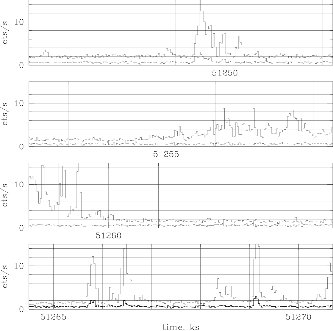 Figure 6.31: An example of the
ACIS background counting rate versus time for a BI chip (S3; top curve) and
an FI chip (I2; bottom curve). These are for the standard grades and
the band from 0.3-10 keV.
Figure 6.31: An example of the
ACIS background counting rate versus time for a BI chip (S3; top curve) and
an FI chip (I2; bottom curve). These are for the standard grades and
the band from 0.3-10 keV.
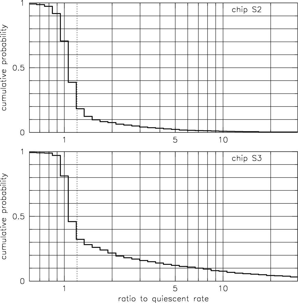 Figure 6.32: An estimate of the
cumulative probability that the ratio of the background counting rate
to the quiescent background counting rate is larger than a given
value. The upper plot is for a representative FI chip (S2) and the lower
plot is for a representative BI chip (S3). The vertical dotted line is a
limiting factor 1.2 used in creating the background data sets.
These probabilities are relevant for the archival data from the first
2-3 years of the mission. After declining with time to almost zero for
a number of years, the amount of flaring has increased with solar maxima,
but there has been less flaring than was seen in the first few
years of the mission.
Figure 6.32: An estimate of the
cumulative probability that the ratio of the background counting rate
to the quiescent background counting rate is larger than a given
value. The upper plot is for a representative FI chip (S2) and the lower
plot is for a representative BI chip (S3). The vertical dotted line is a
limiting factor 1.2 used in creating the background data sets.
These probabilities are relevant for the archival data from the first
2-3 years of the mission. After declining with time to almost zero for
a number of years, the amount of flaring has increased with solar maxima,
but there has been less flaring than was seen in the first few
years of the mission.
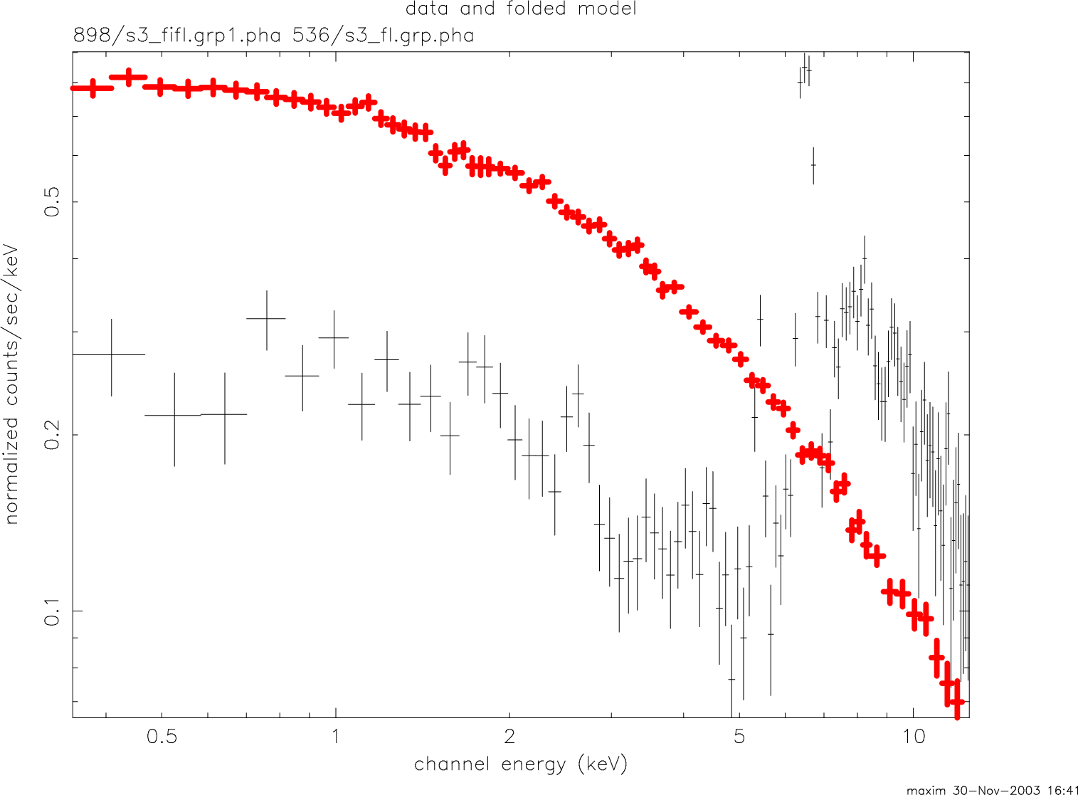 Figure 6.33: Spectra of different background
flares in chip S3. Thick crosses show a common flare species that
affects only the BI chips. Thin crosses show one of the several less
common flare species that affect both the BI and FI chips. Note how
both these spectra are different from the quiescent spectrum (see
Figure 6.29).
Figure 6.33: Spectra of different background
flares in chip S3. Thick crosses show a common flare species that
affects only the BI chips. Thin crosses show one of the several less
common flare species that affect both the BI and FI chips. Note how
both these spectra are different from the quiescent spectrum (see
Figure 6.29).
6.17.4 Background in Continuous Clocking Mode
Apart from compressing the data into one dimension
(Section 6.13.3), there is essentially no difference in the
total background in CC mode and that encountered in the timed exposure
mode. The background per-sky-pixel, however, will be 1024 times
larger, since the sky-pixel is now 1 × 1024 ACIS pixels.
6.18 Sensitivity
The sensitivity for detecting objects is best estimated using the various
proposal tools such as PIMMS, MARX, etc. The "Chandra Proposal
Threads" web page gives detailed examples of how to use
these tools
(https://cxc.harvard.edu/proposer/threads).
6.19 Bright Source X-ray Photon Dose Limitations
Pre-Flight radiation tests have shown that ∼ 200 krads of X-ray
photon dose will damage the CCDs. The mechanism for the
damage is the trapped ionization in the dielectric silicon oxide and
nitride separating the gates from the depletion region. Since the
charge is trapped, the damage is cumulative. Because the structure of
the BI CCDs differs significantly from that of the FI CCDs, the two types of
chips have different photon dose limitations. Specifically, the BI CCDs are more than 25 times as tolerant to a dose of X-ray photons as
compared to the FI CCDs since the former have ∼ 40 μm of bulk Si
protecting the gate layer.
Simulations of astrophysical sources have yielded a very conservative,
spectrally-averaged, correspondence of 100 cts/pix = 1 rad. In this context
`counts' means all photons that impinged on the
detector, whether or not they were piled-up or discarded on-board.
In consultation with the instrument principal investigator (IPI) team, the CXC has adopted the following
mission allowances, per pixel of the two types of chips:
        FI chips:   25 krads    2,500,000 cts/pix
        BI chips: 625 krads  62,500,000 cts/pix
If an observation calls for observing a bright point-like source
close to on-axis, it is suggested that the MARX simulator (with the
parameter DetIdeal=yes & dither, typically, on) be used to calculate whether
the observation may reach 1% of the above mission limits in any one
pixel.
If so, please contact the CXC HelpDesk
(https://cxc.harvard.edu/helpdesk/)
to custom design an observational strategy which may accommodate the
science aims, while maintaining the health & safety of the instrument.
6.20 Limitations on the Number of Required and Optional CCDs
As of 2022-Jan, the ACIS threshold-crossings ("txings") algorithm
is now the primary radiation monitor aboard Chandra. The txings
rates on FI chips are much higher than on BI chips, and the FI
chips are accordingly more sensitive to radiation. Thus,
at least
one FI chip is required for all ACIS observations. This change
has the greatest impact for observers interested in achieving short
frame times using a subarray on S3. The increase in frame time is largest
for an observation which would have been performed on S3-only with a
128-row subarray, but which now requires an additional chip.
In this case, the minimum frame time increases from 0.4 s to 0.5 s.
As of 2025-Nov, S3-only observations are no longer permitted.
Many of the spacecraft components have been reaching
higher temperatures over the course of the mission
because of changes in the insulating layers on the
exterior surfaces of the Chandra spacecraft. The
ACIS electronics and Focal Plane (FP) temperatures can
reach their operational limits depending on the orientation
of the spacecraft and the number of operating CCDs.
The number of operating CCDs and/or the duration
of observations is limited
due to more restrictive thermal constraints.
Starting in Cycle 21,
the proposal submission software allows the proposer to specify
a maximum of 4 required CCDs. If a 5th and/or 6th CCD are
desired by the proposer, they must be specified
as optional at the time of proposal submission.
This restriction is
made necessary due to the difficulty in meeting the thermal
constraints.
Please note that the solar pitch
restrictions specified here, while they correspond to
the pitch range boundaries given in other CXC documents,
are practical representations of more complex physical
behavior and should be understood as approximate.
Several components on the Chandra spacecraft have reached elevated
temperatures at a variety of pitch angles.
Figure 6.34
displays approximate pitch ranges and the components sensitive in
those ranges. Within ACIS, the Power Supply and Mechanism Controller
(PSMC) heats at pitch angles less than 90° and the Focal Plane (FP),
Detector Electronics Assembly (DEA), and Digital Processing Assembly
(DPA) heat at angles larger than 100°.
Observations at pitch angles larger
than about 120°, longer than about 30 ks, and with
5 or 6 CCDs operating are likely to approach or exceed the
DPA and DEA thermal limits
(Figures 6.36
and 6.37).
Finally, the ACIS FP temperature is now most often
several degrees above the desired operating temperature of −119.7 °C,
particularly for observations with pitch angles larger than 100°.
Most of these operating temperatures are reduced by powering fewer CCDs.
Therefore, the Operations team will turn off optional CCDs as required
to optimize ACIS performance and balance thermal constraints (see
section 6.22.1).
For this reason, observations must employ 4 or fewer (required
on) CCDs whenever possible.
Figure 6.35
illustrates the increase in PSMC temperature for
observations at low pitch angles.
Observations using 6 chips are plotted
as green triangles, 5 chips as red circles, and 4 chips as
blue crosses.
Variations in the maximum temperature at a particular pitch
angle and chipset correspond primarily to variations in the starting
temperatures for the observations. The yellow and red lines indicate
the yellow and red limits for the PSMC temperature. It is evident from
Figure 6.35
that using one fewer CCD can reduce the
temperature by a few degrees. In tail-Sun
orientations (pitch angles larger than 100°), the ACIS FP
temperature, the DEA temperature, and the DPA temperature can warm
outside of the desired range. These temperatures can be
reduced by using fewer chips. Roughly speaking, reducing the number of
chips used by one will reduce the asymptotic temperature by a few to
several degrees.
Figure 6.36
displays the DPA temperature as a function of pitch angle for
4, 5, and 6 CCD configurations, and
Figure 6.37
shows the corresponding data for the DEA. The FP temperature as a function of pitch angle for 4, 5, and 6 CCD configurations is shown in
Figure 6.38.
The ACIS PSMC, DEA, DPA and FP temperatures are kept within
operational limits through the
use of thermal models which predict the temperature for a given week,
given the mix and timing of observations. If the predicted temperatures
exceed the planning limits, adjustments are made such as turning off
more optional CCDs, splitting an observation, or rescheduling an
observation at a more favorable pitch angle.
 Figure 6.34: Pitch sensitivity of spacecraft components. Please see Chapter 3 for additional information about the various spacecraft component pitch sensitivities.
 Figure 6.35:
ACIS PSMC temperature as a function of spacecraft pitch angle.
6 CCD observations are indicated by green-filled triangles,
5 CCD observations by red-filled circles and 4 CCD observations are
indicated by blue ×s.
Figure 6.35:
ACIS PSMC temperature as a function of spacecraft pitch angle.
6 CCD observations are indicated by green-filled triangles,
5 CCD observations by red-filled circles and 4 CCD observations are
indicated by blue ×s.
 Figure 6.36:
DPA temperature as a function of spacecraft pitch angle.
6 CCD observations are indicated by green-filled triangles,
5 CCD observations by red-filled circles and 4 CCD observations are
indicated by blue ×s.
Figure 6.36:
DPA temperature as a function of spacecraft pitch angle.
6 CCD observations are indicated by green-filled triangles,
5 CCD observations by red-filled circles and 4 CCD observations are
indicated by blue ×s.
 Figure 6.37:
DEA temperature as a function of spacecraft pitch angle.
6 CCD observations are indicated by green-filled triangles,
5 CCD observations by red-filled circles and 4 CCD observations are
indicated by blue ×s.
Figure 6.37:
DEA temperature as a function of spacecraft pitch angle.
6 CCD observations are indicated by green-filled triangles,
5 CCD observations by red-filled circles and 4 CCD observations are
indicated by blue ×s.
 Figure 6.38:
ACIS FP temperature as a function of spacecraft pitch angle.
6 CCD observations are indicated by green-filled triangles,
5 CCD observations by red-filled circles and 4 CCD observations are
indicated by blue ×s.
Figure 6.38:
ACIS FP temperature as a function of spacecraft pitch angle.
6 CCD observations are indicated by green-filled triangles,
5 CCD observations by red-filled circles and 4 CCD observations are
indicated by blue ×s.
6.21 Observing Planetary and Solar System Objects with ACIS
Chandra has successfully observed several solar system objects, including
Venus, the Moon, Mars, Jupiter, and several comets. Observations of planets
and other solar system objects are complicated because these objects move
across the celestial sphere during an observation and the optical light from
the source can produce a significant amount of charge on the detectors (this
is primarily an issue for ACIS-S observations). Some information regarding
observation planning and data processing is given here. Users are encouraged
to contact the CXC for more detailed help.
6.21.1 The Sun, Earth, and the Moon
Chandra cannot observe the Sun for obvious reasons. Chandra has conducted
observations of the Moon earlier in the mission, but observations of the Moon
with ACIS are currently not allowed. The concern is that the
bright flux of optical and
ultraviolet (UV) photons could potentially polymerize the contaminant on the ACIS filters.
Observations of the dark portion of the Moon are not allowed since there is
a risk that the Sun-illuminated portion of the Moon might encroach upon the
FOV during the observation. For similar reasons, ACIS
observations of Earth (including the dark portion) are not allowed.
See Section 3.3.2 in Chapter 3 and
Chapter 5 for further discussion on avoidances and
constraints.
6.21.2 Observations with ACIS-I
Any solar system object other than the Sun, Earth, the Moon,
and Mercury can be observed with ACIS-I, subject to the avoidances
discussed in Section 3.3.2 and Chapter 5.
Previous solar system
observations with ACIS-I have not
revealed significant contamination from optical light. However, proposers
are encouraged to work with the CXC when planning the specifics of a
given observation. Since the source moves across the celestial sphere in
time, an image of the event data will exhibit a "streak" associated with
the source. The CIAO tool sso_freeze can be used to
produce an event data file with the motion of the source removed.
6.21.3 Observations with ACIS-S
Any solar system object other than the Sun, Earth, the Moon,
and Mercury can be observed with ACIS-S, subject to the avoidances
discussed in Section 3.3.2 and Chapter 5.
The ACIS-S array can be used with or without a grating.
The BI CCDs are more
sensitive to soft X-rays than the ACIS-I array CCDs,
but the entire ACIS-S array
suffers from the disadvantage that its OBF is thinner than for ACIS-I and
may transmit a non-negligible flux of visible light onto the CCDs. It is
thus necessary to estimate the amount of charge produced in the CCDs due to
the optical light. More detailed information can be found at
https://cxc.harvard.edu/cal/Hrma/UvIrPSF.html
and from the CXC via HelpDesk
(https://cxc.harvard.edu/helpdesk/).
If the optical light leak is small enough, it can be mitigated by simply
shortening the frame time. This leads to a linear drop in the number of ADU
due to optical light. If possible, VF mode should be used, since in this
mode the outer 16 pixels of the 5×5 region allows a "local"
bias to be subtracted from the event to correct for any possible light
leakage. However,
see the warnings in Section 6.15.2.
The optical light also invalidates the bias taken at the beginning of the
observation if a bright planet is in the field. It is therefore desirable
to take a bias frame with the source out of the field of view. This bias
map is useful even when processing 5×5 pixels in VF mode since it can be
employed as a correction to the local average "bias" computed from the
16 outer pixels, thereby correcting for hot pixels, cosmetic defects etc.
A more sophisticated approach to dealing with excess charge due to optical
light is to make an adjustment to the event and split thresholds. Event
grades are described in more detail in Section 6.15.1. Excess charge (in
ADU) due to optical light will be added to the event and split counters
on-board. Without an adjustment to the thresholds (or a large enough
threshold), many of the X-ray events may have all nine pixels of a
3×3 pixel event detection cell above the split threshold, in which case
the event will not be telemetered to the ground. If the adjustment is too
large, X-ray events may not be detected because they may not exceed the
event threshold.
Users should be aware that if the detection thresholds are adjusted,
standard CXC processing of planetary data will give inaccurate estimates
of event pulse heights and grades. To analyze such data, a thorough
understanding of the energy calibration process and manual massaging of
the data will be required.
6.22 Observing with ACIS-the Input Parameters
This section describes the various inputs that either must be, or can
be, specified to perform observations with ACIS. The
subsections are organized to match the Chandra Proposal Software (CPS)
form at https://cxc.harvard.edu/proposer/CPS.html and includes implications
of the possible choices. As
emphasized at the beginning of the Chapter, ACIS is moderately
complex and the specific characteristics of the CCDs and their
configuration in the instrument lead to a number of alternatives for
accomplishing a specific objective-detailed trade-offs are the
responsibility of the observer. For example, it might seem obvious that
observations of a faint point source may be best accomplished by
selecting the ACIS-S array with the aim point on S3, the BI device
that can be placed at the best focus of the telescope, and the
CCD with the best average energy resolution. On the other hand,
perhaps the science is better served by offset pointing (by a few
arcmin) the target onto S2, very near to the frame store, where the
FI energy resolution is better than that of S3. Or,
if the object is very faint-so that the total number of
photons expected is just a handful (not enough to perform any
significant spectroscopy)-the advantage of S3 may not be so
obvious considering the smaller field of view and its higher
background rate, and perhaps the ACIS-I array, which would optimize
the angular resolution over a larger field, may be more attractive.
6.22.1 Required Parameters
Some ACIS input parameters must be specified: the number and
identity of the CCDs to be used, the Exposure Mode, and the Event
Telemetry Format. For imaging observations using
ACIS-I or ACIS-S with no grating, the maximum number of counts expected
to be used in a spectral analysis of the source(s) must be supplied.
If pile-up and telemetry saturation are not
expected to be a problem for the observation, then these are the only
parameters that need to be specified.
Number and Choice of CCDs
The CPS requires the observer to specify the desired aimpoint and to
identify the CCDs they want to use.
Prior to Cycle 13, the use of 6 CCDs was encouraged to facilitate
serendipitous detections. Starting in Cycle 20,
the CPS limits the number of CCDs that may be specified as required to
a maximum of 4
for thermal reasons. The proposer may specify additional optional
CCDs to bring the total of required plus optional CCDs to as many as
6 CCDs, but the proposer should be aware that optional CCDs may be
turned off.
If the science objectives of the proposal require 5 or 6 CCDs, the proposer must work with their Chandra Uplink Support Scientist after the proposal is selected in order to specify a 5th or 6th CCD as required.
But proposers should be aware that 5 or 6 CCD observations
are more difficult to schedule and are more likely to be
split into multiple short observations if the exposure is long.
Using fewer CCDs is beneficial in keeping the ACIS electronics and the ACIS focal plane (FP) temperatures
within the required operating ranges. See Section 6.20
for further information on thermal limitations and selection
requirements for ACIS and the number of operating CCDs.
The selection of CCDs on the CPS form is discussed in the next section.
Choosing Optional CCDs & Optional CCD Policy
The observer may specify that a given CCD must be on for an
observation by entering "Y"
for that CCD at the appropriate place in the CPS form. If there are
CCDs that the observer does not require for their science, they should
enter "N." If there are CCDs that the observer would prefer to have
turned on should thermal conditions allow it, the rank-ordered
designations "OFF1," "OFF2," up to "OFF5" should be used.
The CCD designated as "OFF1" would be the first one to be turned off,
and the CCD designated as "OFF5" would be the last that would be
turned off.
Even if the science requires 5 or 6 CCDs,
the observer must set the designation for the four most useful
as "Y" and the least useful CCD(s) to
optional status "OFF1" ("OFF2"). In these instances, the proposer
should include a comment in the CPS form that 5 or 6 CCDs are required
for the science. If the proposal is accepted, the observer may work
with their Chandra Uplink Support Scientist to change "OFF1" ("OFF2")
to "Y." The CXC will make its best effort to try to schedule the
observation under the appropriate thermal conditions. The observer
should discuss the configuration with Uplink Support and, if there are
difficulties in assessing which CCDs should be optional, please contact
the CXC HelpDesk
(https://cxc.harvard.edu/helpdesk/).
Should it be possible to accommodate the observer's request
for 5 or 6 CCDs, the observation will most likely
take place at solar pitch angles less than 130°.
Recommended Chip Sets
Observers should specify the chip set that is
best for their primary science. The following suggestions have proven
to be popular and would facilitate a more useful and homogeneous
archive. Given the current thermal performance of the spacecraft, it is
possible that any number of optional CCDs would be turned off.
Some Recommended Chip Sets: ACIS-I Aimpoint (Imaging)
The rationale for the first ACIS-I imaging configuration
(Figure 6.39) is that, in the
unlikely event of major background flares, telemetry
might saturate more rapidly if S3 were on. In addition, since S2 is
further from the ACIS-I aimpoint on I3, data on S2 may provide nearby
local (FI) background if the target contains diffuse emission which does not
extend as far as S2.
For the second ACIS-I imaging configuration
(Figure 6.40),
the rationale is that S3 is generally more sensitive and closer to
the ACIS-I aimpoint, and so more sensitive to serendipitous source
detection.
The rationale for the third ACIS-I imaging configuration
(Figure 6.41)
is that it is desired to have both S2 and S3 on, but it is not
required. The CCD specified "OFF1" would be the first to be turned off.
Some Recommended Chip Sets: ACIS-S Aimpoint (Imaging)
For deciding on chipsets for ACIS-S imaging, several factors come into play. In general, chips closest to
the S3 aimpoint would be selected as required, while
those farthest from the aimpoint (where the PSF is degraded) would be selected as optional.
The first ACIS-S imaging configuration (Figure 6.42) is the basic default ACIS-S configuration. The aimpoint is on S3, a BI chip. If a BI chip is used, it is required that an FI chip also be on in order to provide more reliable monitoring of the radiation environment. S2 has several advantages as an FI chip to be used with the S3 aimpoint, notably that is closest to the S3 aimpoint, providing relatively good imaging performance. With only two required CCDs powered on, the focal plane heating is reduced.
If a larger field of view is needed, up to six total chips can be specified as potentially on, of which only a maximum of four can be set as required. That is, a setup with four required chips could have up to two optional chips (tagged as "OFF1" and "OFF2"). As noted above, thermal constraints may require that optional chips be turned off.
The rationale for the second ACIS-S imaging configuration
(Figure 6.43) is that the optional S1 and S4 allow for the possibility of a larger imaging area, and S4 is preferred over S1 if one chip must be dropped: if necessary, S1 will be turned off first. Thermal constraints may require one or both of the optional chips be turned off.
The rationale for the third ACIS-S imaging configuration
(Figure 6.44) is that the optional S1 and S4 allow for the possibility of larger imaging area. As having S1 on allows the S3 background spectrum to be modeled if
diffuse emission covers all or part of S3,
S1 is preferred over S4 in the situation that thermal constraints require a single chip must be dropped. If it important to the science that S1 be available for this purpose, the user should instead specify a configuration with three required chips (S3+S2+S1).
The rationale for the fourth ACIS-S imaging configuration
(Figure 6.45) is that the optional I2 allows for the possibility of larger imaging area. S1
will have a higher count rate than an FI CCD in the event of
a background flare and thus it might be desirable to turn S1
off.
The rationale for the fifth ACIS-S imaging configuration
(Figure 6.46)
is that the observer may want to use S1 to model the background on S3, and it is desirable to have S4 turned off. S4 also has significant noise streaks with resulting decreased sensitivity, so some users may prefer to specify I2 as optional instead of S4.
The rationale for the sixth ACIS-S imaging configuration
(Figure 6.47) is that for this observation
it would be desirable to have 6 CCDs on. It is
probable that one or two optional CCDs would be turned off.
Recommended Chip Set: ACIS-S Aimpoint (Spectroscopy)
The optimum
ACIS-S spectroscopy chip set depends strongly on the expected spectrum
of the target. Typically the maximum signal is desired, so the HETG and
LETG observer is most likely to request 6 ACIS-S chips (with at most
4 specified "ON"). If the science does depend strongly
on the flux received on the S0 and S5
CCDs, the observer would need to work with their Chandra Uplink Support
Scientist to specify all 6 ACIS-S CCDs as required on
(see Figure 6.48). However, the
observer should be aware that the amount of useful
flux on S0 and S5 with the LETG is typically quite low given they are
both FI CCDs (see Figure 9.6) and also
because of the loss due to the optical blocking filter contamination layer.
ACIS Counts Information
Proposers not using gratings are asked for the maximum number of counts expected from the brightest source to be analyzed in their observation. This answer is used by mission planners to schedule observations during the proper thermal conditions for the perceived science goals. If the proposer is interested in the optimal spectral performance of the ACIS CCDs, they should seriously consider using the minimum number of CCDs necessary for their science goals. See also Section 6.22.5 for information on "warm" ACIS operations.
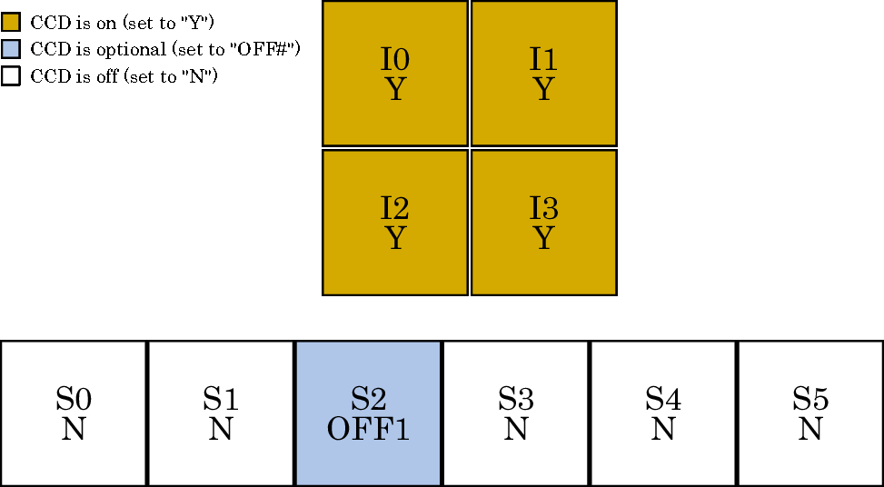 Figure 6.39: ACIS-I imaging, nominal I3 aimpoint (4 Required CCDs, 1 Optional CCD)
 Figure 6.40: ACIS-I imaging, nominal I3 aimpoint (4 Required CCDs, 1 Optional CCD)
 Figure 6.41: ACIS-I imaging, nominal I3 aimpoint (4 Required CCDs, 2 Optional CCDs)
 Figure 6.42: ACIS-S imaging, nominal S3 aimpoint (2 Required CCDs)
 Figure 6.43: ACIS-S imaging, nominal S3 aimpoint (2 Required CCDs, 2 optional CCDs)
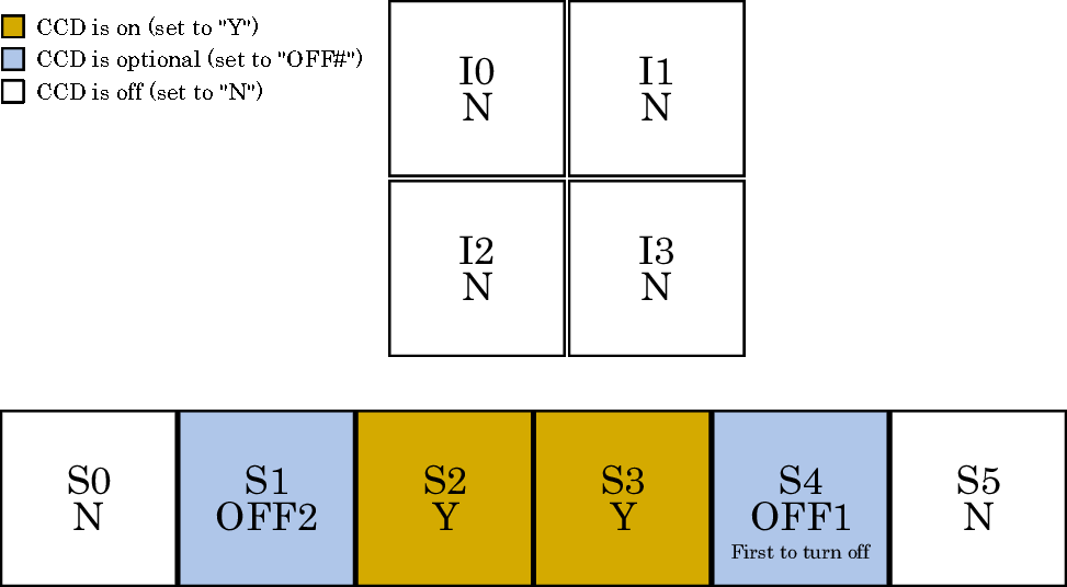 Figure 6.44: ACIS-S imaging, nominal S3 aimpoint (2 Required CCDs, 2 optional CCDs)
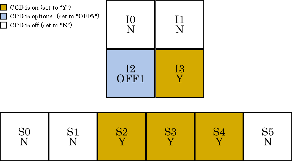 Figure 6.45: ACIS-S imaging, nominal S3 aimpoint (4 Required CCDs, 1 Optional CCD)
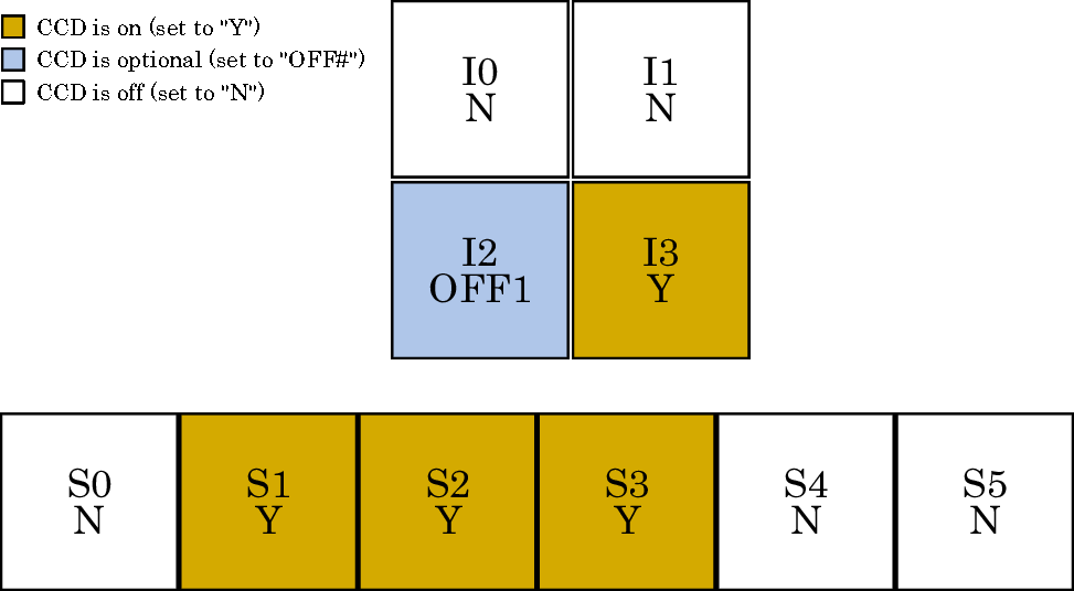 Figure 6.46: ACIS-S imaging, nominal aimpoint (4 Required CCDs, 1 Optional CCD)
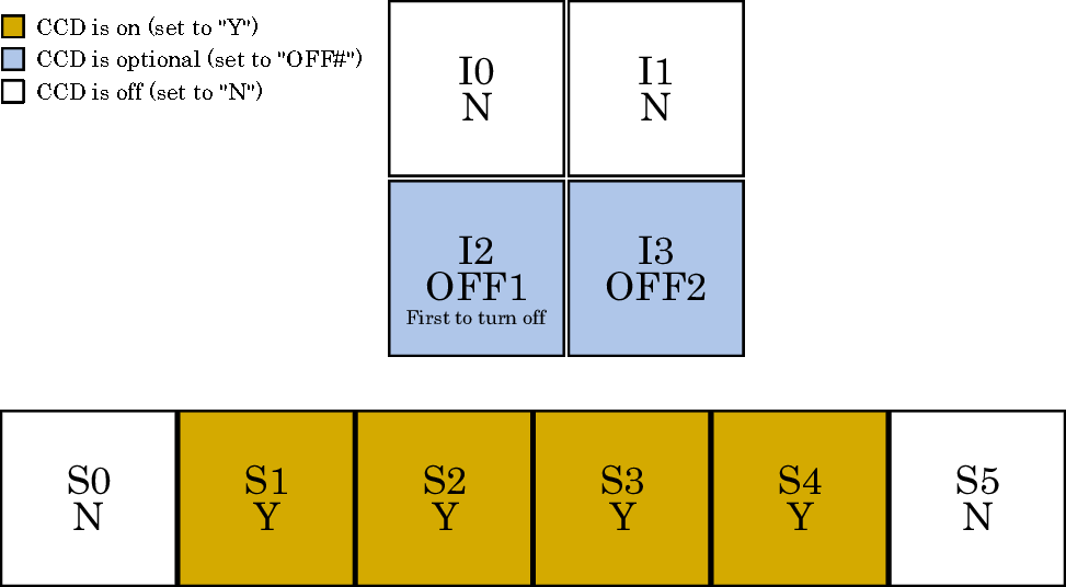 Figure 6.47: ACIS-S imaging, nominal aimpoint (4 Required CCDs, 2 Optional CCDs)
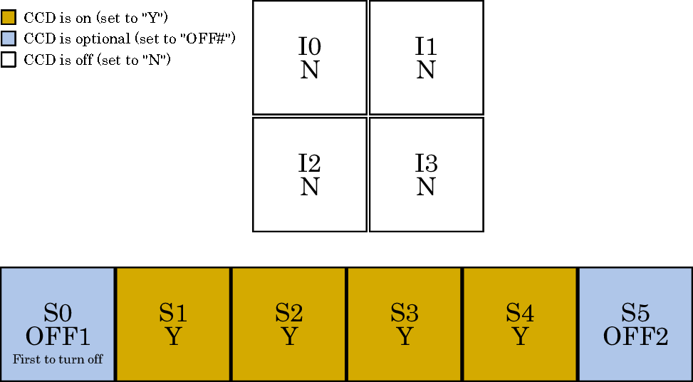 Figure 6.48: ACIS-S spectroscopy, nominal aimpoint (4 Required CCDs, 2 Optional CCDs)
Optional Parameters that affect Pile-Up
See Section 6.13.1 for information on how the selection
of the number of operating CCDs and the size and position of the
subarray affects the minimum frame time. In general, using
fewer CCDs will permit a faster read-out. For example, using
the smallest subarray of 128 rows in the middle of I-array CCDs gives
a minimum frame time of 0.5 s with 1 CCD operating and a minimum
frame time of 0.7 s with 6 CCDs operating. In almost all cases,
the observer should leave the parameter on the CPS target
form that asks if the most efficient frame time should be
used at the default value of "Y." This parameter should
be changed only if the observer fully understands the impact on
efficiency of their observation. Please contact the
CXC HelpDesk (https://cxc.harvard.edu/helpdesk/) if you are considering a non-default setting
and are unsure of the CCD selection and CCD Frame exposure
time to use.
Exposure Mode
There are only two choices: Timed Exposure (TE) mode
(see Section 6.13.1)
or Continuous Clocking (CC) mode (see Section 6.13.3).
Timed Exposure Mode
The Timed Exposure (TE) mode with the default nominal (and optimal) frame
time of 3.2s is the typical mode for ACIS observations. Note that the
option of selecting frame times shorter than nominal reduces observing
efficiency, and hence the number of photons collected for a given
observation time. (Note that the value of the nominal frame time
can differ a bit from 3.2s depending on how many CCDs are used; see
Section 6.13.1.)
Continuous Clocking Mode
The Continuous Clocking (CC) mode is useful when timing data are so
critical and/or pile-up is such a problem that the sacrifice of one
dimension of spatial data is warranted. The use of continuous clocking
may also lead one to consider specifying a particular satellite roll
orientation (see Chapter 3) to avoid having two
different sources produce events in the same CCD column. (See also
Section 6.22.4 below.)
Figure 6.48: ACIS-S spectroscopy, nominal aimpoint (4 Required CCDs, 2 Optional CCDs)
Optional Parameters that affect Pile-Up
See Section 6.13.1 for information on how the selection
of the number of operating CCDs and the size and position of the
subarray affects the minimum frame time. In general, using
fewer CCDs will permit a faster read-out. For example, using
the smallest subarray of 128 rows in the middle of I-array CCDs gives
a minimum frame time of 0.5 s with 1 CCD operating and a minimum
frame time of 0.7 s with 6 CCDs operating. In almost all cases,
the observer should leave the parameter on the CPS target
form that asks if the most efficient frame time should be
used at the default value of "Y." This parameter should
be changed only if the observer fully understands the impact on
efficiency of their observation. Please contact the
CXC HelpDesk (https://cxc.harvard.edu/helpdesk/) if you are considering a non-default setting
and are unsure of the CCD selection and CCD Frame exposure
time to use.
Exposure Mode
There are only two choices: Timed Exposure (TE) mode
(see Section 6.13.1)
or Continuous Clocking (CC) mode (see Section 6.13.3).
Timed Exposure Mode
The Timed Exposure (TE) mode with the default nominal (and optimal) frame
time of 3.2s is the typical mode for ACIS observations. Note that the
option of selecting frame times shorter than nominal reduces observing
efficiency, and hence the number of photons collected for a given
observation time. (Note that the value of the nominal frame time
can differ a bit from 3.2s depending on how many CCDs are used; see
Section 6.13.1.)
Continuous Clocking Mode
The Continuous Clocking (CC) mode is useful when timing data are so
critical and/or pile-up is such a problem that the sacrifice of one
dimension of spatial data is warranted. The use of continuous clocking
may also lead one to consider specifying a particular satellite roll
orientation (see Chapter 3) to avoid having two
different sources produce events in the same CCD column. (See also
Section 6.22.4 below.)
6.22.2 Optional Parameters
Alternating Exposures
This option applies only to Timed Exposure (TE) mode. The parameters
specifying an alternating exposure are:
- the number of secondary exposures per primary exposure (1-15)
- the primary exposure frame time
Frame times and efficiencies in TE mode are discussed in
Section 6.13.1, and the Alternating
Exposure option is discussed in Section 6.13.2.
Energy Filtering
It is possible to remove events from the telemetry stream, and thus
avoid telemetry saturation, by specifying an energy acceptance filter
within which detected events will be telemetered. The default discards
events above 3250 ADU (nominally 13 keV). The total per-chip
background rates for different upper energy cut-offs are in
Table 6.10.
Starting 2006-Sep, a new PHA to energy conversion is used for
observations with energy filters. Two sets of conversions are
used, depending on the aimpoint of the observation. Observations with
ACIS-S at the aimpoint use a conversion tailored for the
BI CCDs and those with ACIS-I at the aimpoint use
FI CCD-specific conversions. The BI and FI specific
conversions are more accurate for each type of CCD than the conversion
used in previous cycles. The assumption is that it is desirable to have
the most accurate gain conversion for the CCD on which the
HRMA default aimpoint falls. Note that the conversion only impacts the on-orbit
energy filtering. Ground data processing
will always apply the appropriate PHA to energy conversion.
The observer should be aware that for observations which mix CCD types
(i.e. both BI and FI CCDs on), the selected
conversion (based on aimpoint
as above), will nevertheless apply to all selected CCDs. This will
not affect the
observation if the low energy threshold for the energy filter (the
"Event filter: Lower" parameter) is 0.5 keV or less, as the use of
either conversion at these energies results in essentially no
difference in the number of accepted events. However, for selection
of a low energy threshold above 0.5 keV, the
conversions are significantly different.
Proposers who need an energy filter lower limit above
0.5 keV are encouraged to contact the CXC HelpDesk
(https://cxc.harvard.edu/helpdesk/)
to discuss their
plans with an instrument scientist.
Spatial Windows
A more sophisticated approach to removing data from the telemetry
stream, and thus avoiding telemetry saturation, is by the use of a
Spatial Window. This option offers a good deal of flexibility. One may
define up to 6 Spatial Windows per CCD. Each window can be placed
anywhere on the chip. Note there is a significant difference between
a Spatial Window and a Subarray (Section 6.13.1):
Subarrays affect the transmission of CCD data to the on-board
ACIS processors; Spatial Windows select events detected by the processors
and only telemeters a filtered subset of events. The user may also specify the
window energy threshold and energy range.
Spatial windows can specify the sample rate for events inside them.
A sample rate of 0 excludes all events; the default rate of 1
includes all events; a rate of n > 1 telemeters one out of every
n events in the window. As one example of a use case, a spatial window
could be used to eliminate
a bright, off-axis source that would otherwise overwhelm the
telemetry stream. The order in which the spatial windows are
specified is important if they overlap. The first specified
window which includes a given pixel will be applied to events at that
pixel.
6.22.3 Non-ACIS Parameters Relevant to an Observation with ACIS
There are a small number of additional parameters that need to be
considered in specifying an observation with ACIS: (1) the off-axis
pointing (if required), which reduces the flux, and spreads out the
image; (2) the roll angle (Chapter 4); (3) time
constraints (if any); and (4) time monitoring intervals (if
any).
6.22.4 Choosing CC Mode for Bright Source Observation
The Continuous Clocking (CC) mode (see Section 6.13.3) can
be used, with or without gratings, to mitigate pile-up of
very bright sources (see Section 6.16.2).
CC mode has two standard telemetry formats:
"faint" and "graded." Faint mode retains the event-island
information needed for the application of the CTI correction
but requires a larger data volume per event compared to
graded mode. Thus, graded mode is less likely to saturate
telemetry but spectral features needing CTI correction cannot
be recovered. Note, however, that gratings can be used to
further reduce throughput while also preserving discrete spectral
structures such as emission and absorption lines and edges in
the dispersed spectrum regardless of telemetry format.
The calibrations of TE and CC modes are very similar and only
small differences are present with respect to ACIS gain, response,
and integrated grade distribution, with CC faint mode versus CC
graded mode choice resulting in less than 3% differences at the most.
Starting in 2009-Nov, the CC faint and
graded modes have been altered to include some of the flight grades
that were previously rejected on-board: ACIS now telemeters all
flight grades except 24, 107, 127, 214, 223, 248, 251, 254, and 255.
It is recommended to use graded mode only in extreme cases.
See Section 8.5.2 in
Chapter 8 for for recommended ACIS modes, CCD choices,
subarrays, etc; that section also discusses some aspects
of analyzing the data.
6.22.5 Warm ACIS Observations
Proposers should consider the following options to ensure the lowest possible focal plane temperature during their observation:
- minimizing the number of CCDs so as to reduce the potential for
thermally-induced gain drifts that might broaden lines over long
observations
- locating targets near the frame store regions
(low CHIPY) using offset pointing (see Chapter 3) to maximize energy resolution (see Figures 6.14
and 6.15) and/or
- using the BI chip S3, which has a more spatially-uniform energy
resolution across the CCD and better energy resolution than the
FI chips at high CHIPY values.
Warm FP temperatures do not affect ACIS imaging capabilities.
Thus, proposed science goals that do not require precision spectroscopy need
not be concerned with FP temperature.
Since 2020, Mission Planners have used the user-supplied source count information to help identify proposed observations that do not have high precision spectroscopy as a science goal and thus may be observed at warmer focal plane temperatures, which can reduce the need to split an observation.
For observations using HETG (or LETG) and ACIS the impact of higher FP
temperatures is insignificant since the energy calibration is based on the
position of the event in the dispersed spectrum.
Accordingly, HETG observations may also be conducted at warm FP temperatures.
(Note, however, imaging spectroscopy for the zero-order will be affected by
warmer temperatures.)
|